INDUSTRIAL TEMPERATURE RANGE
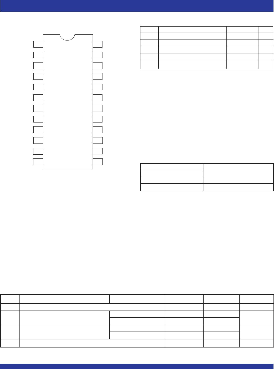
IDT74CBTLV3861
LOW-VOLTAGE 10-BIT BUS SWITCH
3
Symbol Parameter Test Conditions Min. Typ.
(1)
Max. Unit
VIK Control Inputs, Data I/O VCC = 3V, II = –18mA — — –1.2 V
II Control Inputs, Data I/O VCC = 3.6V, VI = VCC or GND — — ±1 μA
IOZ Data I/O VCC = 3.6V, VO = 0 or 3.6V, switch disabled — — 5 μA
IOFF VCC = 0, VI or VO = 0 to 3.6V — — 50 μA
ICC VCC = 3.6V, IO = 0, VI = VCC or GND — — 10 μA
ΔICC
(2)
Control Inputs VCC = 3.6V, one input at 3V, other inputs at VCC or GND — — 300 μA
CI Control Inputs VI = 3V or 0 — 4 — pF
CIO(OFF) VO = 3V or 0, OE = VCC —6 —pF
V
CC = 2.3V VI = 0 IO = 64mA — 5 8
Typ. at VCC = 2.5V IO = 24mA — 5 8
R
ON
(3)
VI = 1.7V IO = 15mA — 27 40 Ω
V
I = 0 IO = 64mA — 5 7
VCC = 3V IO = 24mA — 5 7
VI = 2.4V IO = 15mA — 10 15
DC ELECTRICAL CHARACTERISTICS OVER OPERATING RANGE
Following Conditions Apply Unless Otherwise Specified:
Operating Conditions: TA = –40°C to +85°C
VCC = 2.5V ± 0.2V VCC = 3.3V ± 0.3V
Symbol Parameter Min. Max. Min. Max. Unit
t
PD
(1)
Propagation Delay − 0.15 − 0.25 ns
A to B or B to A
tEN Output Enable Time 1 4.5 1 4.2 ns
OE to A or B
tDIS Output Disable Time 1 5 1 5 ns
OE to A or B
NOTE:
1. The propagation delay is the calculated RC time constant of the typical on-state resistance of the switch and the specified load capacitance driven by an ideal voltage source
(zero output impedance).
SWITCHING CHARACTERISTICS
NOTES:
1. Typical values are at VCC = 3.3V, +25°C ambient.
2. The increase in supply current is attributable to each current that is at the specified voltage level rather than VCC or GND.
3. This is measured by the voltage drop between the A and B terminals at the indicated current through the switch.