Nexperia
74AHC9541A
Octal buffer/line driver; 3-state
74AHC9541A All information provided in this document is subject to legal disclaimers. © Nexperia B.V. 2017. All rights reserved.
Product data sheet Rev. 1 — 28 June 2017
10 / 17
Table 8. Noise characteristics
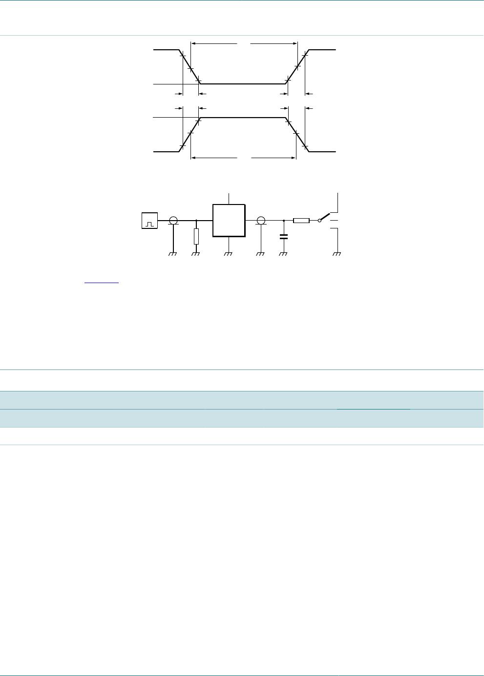
GND = 0 V. For test circuit see Figure 7.
T
amb
= 25 °CSymbol Parameter Conditions
Min Typ Max
Unit
V
CC
= 3.3 V; C
L
= 50 pF
V
OL(p)
LOW-level output voltage (peak) - 0.2 0.8 V
V
OL(v)
LOW-level output voltage (valley) -0.8 -0.1 - V
V
OH(v)
HIGH-level output voltage (valley) - 3.0 - V
V
IH(AC)
AC HIGH-level input voltage 2.31 - - V
V
IL(AC)
AC LOW-level input voltage - - 0.99 V
V
CC
= 5.0 V; C
L
= 50 pF
V
OL(p)
LOW-level output voltage (peak) - 0.5 1.5 V
V
OL(v)
LOW-level output voltage (valley) -1.5 -0.3 - V
V
OH(v)
HIGH-level output voltage (valley) - 4.5 - V
V
IH(AC)
AC HIGH-level input voltage 3.5 - - V
V
IL(AC)
AC LOW-level input voltage - - 1.5 V
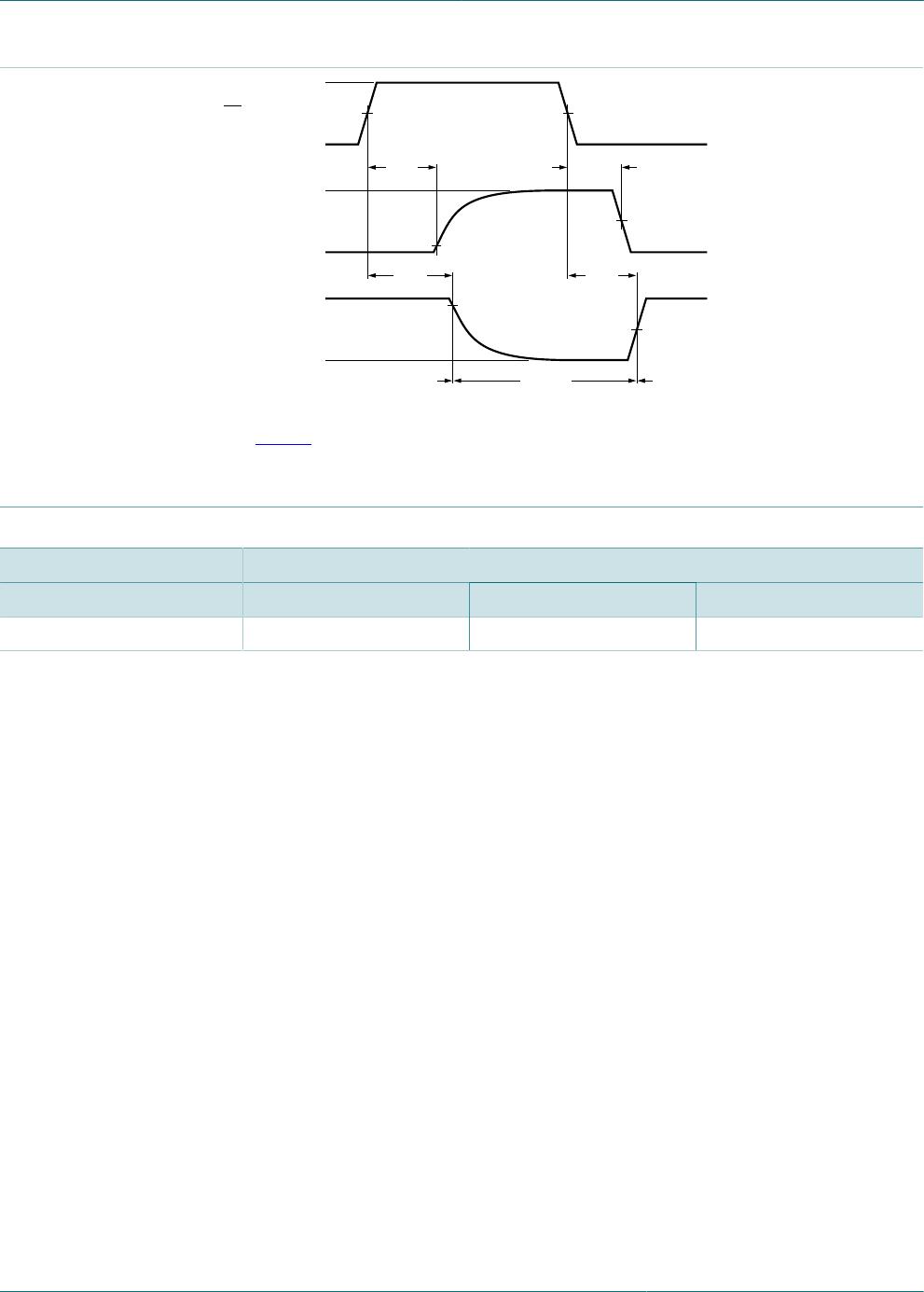
10.1 Waveforms and test circuit
aaa-026895
Yn output
An, S input
t
PHL
t
PLH
V
M
V
M
V
I
GND
V
OH
V
OL
V
M
V
M
t
PHL
V
M
t
PLH
V
M
Yn output
V
OH
V
OL
Measurement points are given in Table 9.
V
OL
and V
OH
are typical voltage output levels that occur with the output load.
Figure 5. Propagation delay input (An, S) to output (Yn)