©2014 Silicon Storage Technology, Inc. DS20005053B 04/14
10
4 Mbit (x16) Multi-Purpose Flash Plus
SST39VF401C / SST39VF402C / SST39LF401C / SST39LF402C
Data Sheet
Data Protection
The SST39VF401C/402C and SST39LF401C/402C provide both hardware and software features to pro-
tect nonvolatile data from inadvertent writes.
Hardware Data Protection
Noise/Glitch Protection: A WE# or CE# pulse of less than 5 ns will not initiate a write cycle.
V
DD
Power Up/Down Detection: The Write operation is inhibited when V
DD
is less than 1.5V.
Write Inhibit Mode: Forcing OE# low, CE# high, or WE# high will inhibit the Write operation. This pre-
vents inadvertent writes during power-up or power-down.
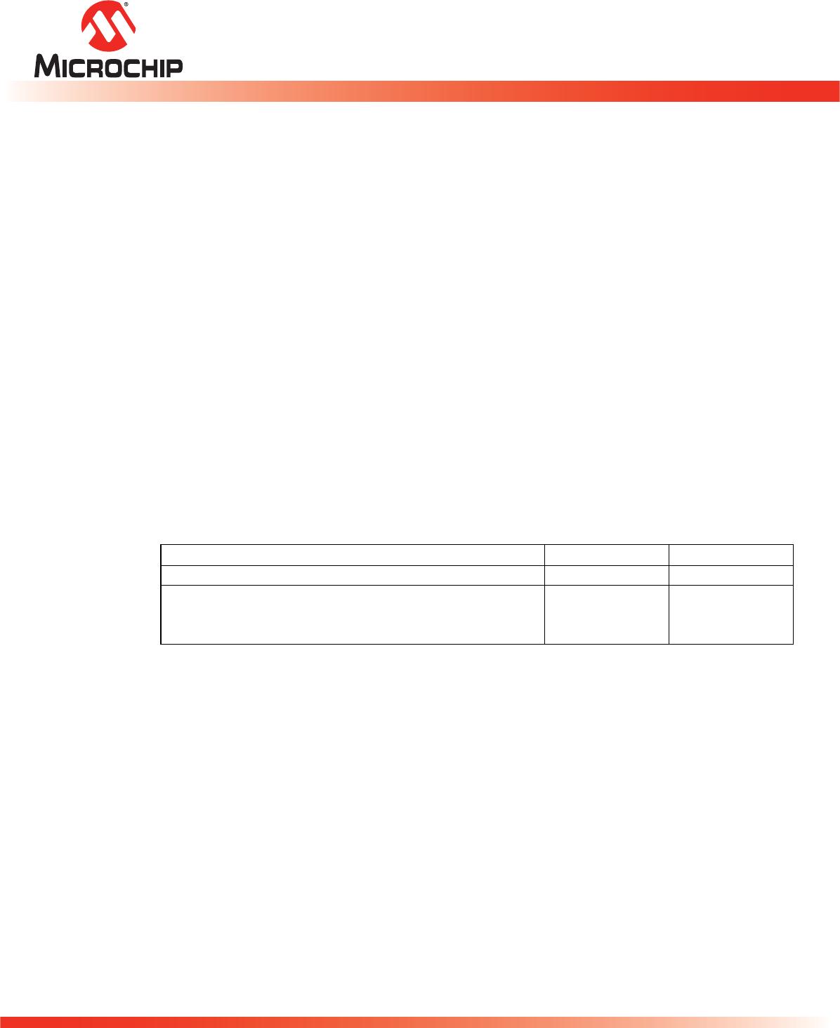
Hardware Block Protection
The SST39VF402C/SST39LF402C support top hardware block protection, which protects the top 8
KWord block of the device. The SST39VF401C/SST39LF401C support bottom hardware block protec-
tion, which protects the bottom 8KWord block of the device. The Boot Block address ranges are
described in Table 4. Program and Erase operations are prevented on the 8 KWord when WP# is low.
If WP# is left floating, it is internally held high via a pull-up resistor, and the Boot Block is unprotected,
enabling Program and Erase operations on that block.
Hardware Reset (RST#)
The RST# pin provides a hardware method of resetting the device to read array data. When the RST#
pin is held low for at least T
RP,
any in-progress operation will terminate and return to Read mode. When
no internal Program/Erase operation is in progress, a minimum period of T
RHR
is required after RST#
is driven high before a valid Read can take place (see Figure 18).
The Erase or Program operation that has been interrupted needs to be re-initiated after the device
resumes nor mal operation mode to ensure data integrity.
Software Data Protection (SDP)
The SST39VF401C/402C and SST39LF401C/402C provide the JEDEC approved Software Data Pro-
tection scheme for all data alteration operations, i.e., Program and Erase. Any Program operation
requires the inclusion of the three-byte sequence. The three-byte load sequence is used to initiate the
Program operation, providing optimal protection from inadvertent Write operations, e.g., during the
system power-up or power-down. Any Erase operation requires the inclusion of six-byte sequence.
These devices are shipped with the Software Data Protection permanently enabled. See Table 7 for
Table 4: Boot Block Address Ranges
Product Address Range
Bottom Boot Block
SST39VF401C/SST39LF401C 00000H - 01FFFH
Top Boot Block
SST39VF402C/SST39LF402C 3E000H - 3FFFFH
T4.0 25053