©2014 Silicon Storage Technology, Inc. DS20005053B 04/14
19
4 Mbit (x16) Multi-Purpose Flash Plus
SST39VF401C / SST39VF402C / SST39LF401C / SST39LF402C
Data Sheet
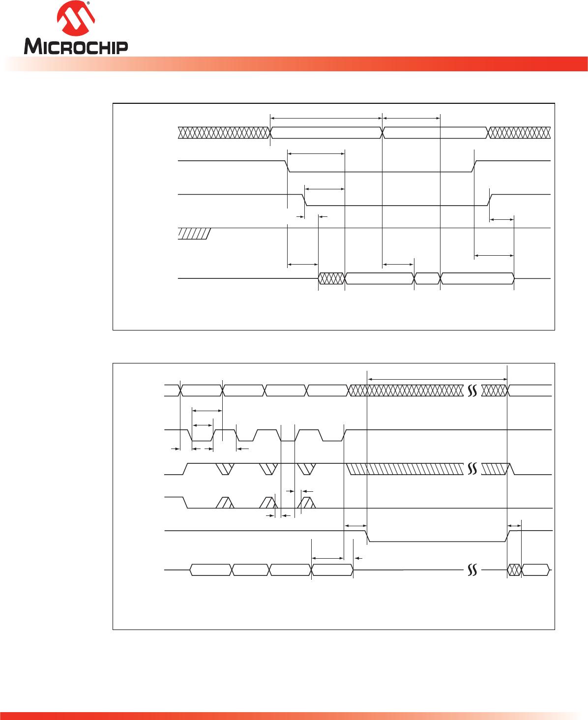
AC Characteristics
Table 17: Read Cycle Timing Parameters - V
DD
= 3.0-3.6V for SST39LF401C/402C and
2.7-3.6V for SST39VF401C/402C
Symbol Parameter
SST39VF401C/402C SST39LF401C/402C
UnitsMin Max Min Max
T
RC
Read Cycle Time 70 55 ns
T
CE
Chip Enable Access Time 70 55 ns
T
AA
Address Access Time 70 55 ns
T
OE
Output Enable Access Time 35 30 ns
T
CLZ
1
1. This parameter is measured only for initial qualification and after a design or process change that could affect this parameter .
CE# Low to Active Output 0 0 ns
T
OLZ
1
OE# Low to Active Output 0 0 ns
T
CHZ
1
CE# High to High-Z Output 20 15 ns
T
OHZ
1
OE# High to High-Z Output 20 15 ns
T
OH
1
Output Hold from Address Change 0 0 ns
T
RP
1
RST# Pulse Width 500 500 ns
T
RHR
1
RST# High before Read 50 50 ns
T
RY
1,2
2. This parameter applies to Sector-Erase, Block-Erase and Program operations.
This parameter does not apply to Chip-Erase operations.
RST# Pin Low to Read Mode 20 20 µs
T17.3 25053
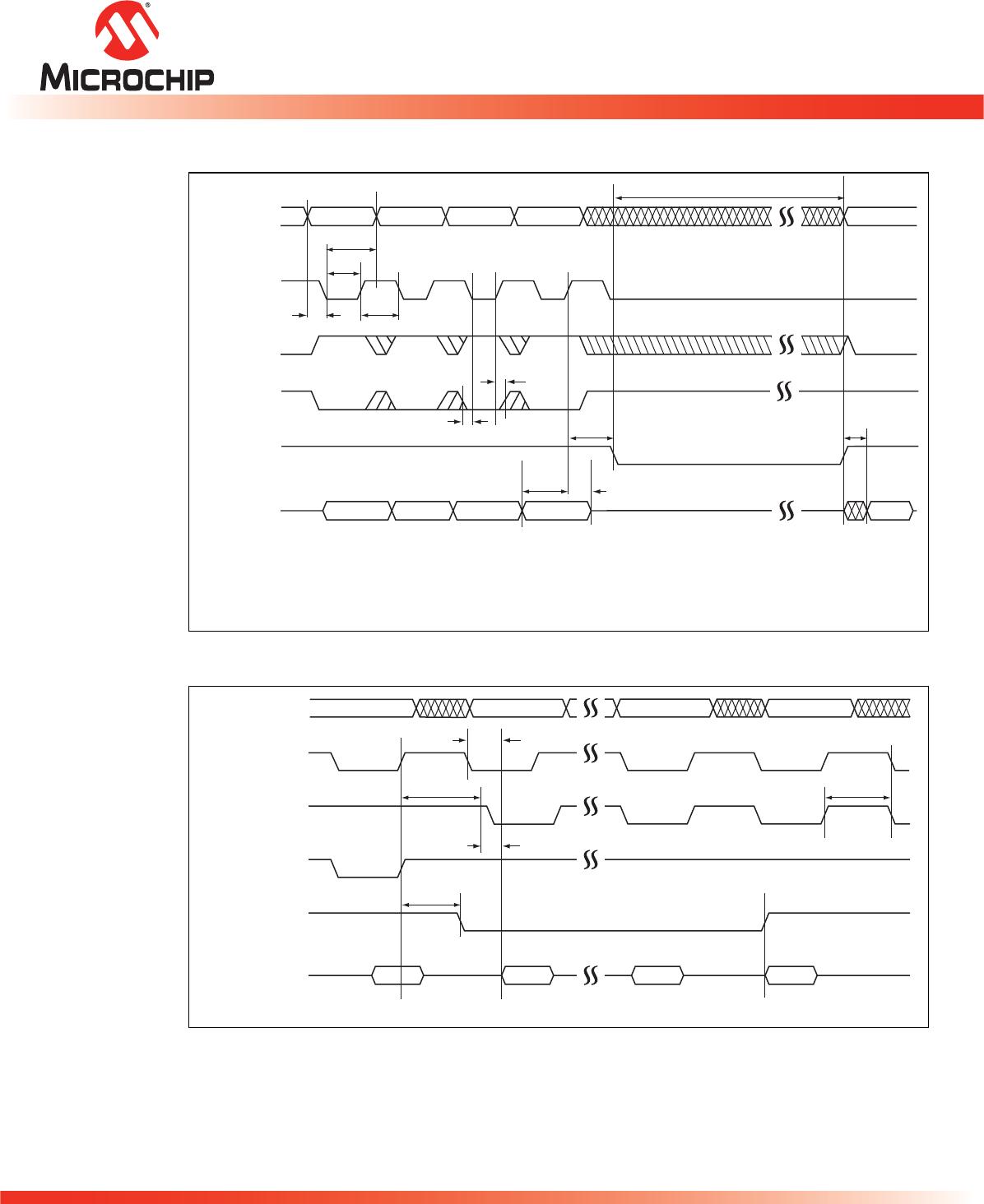
Table 18: Program/Erase Cycle Timing Parameters
Symbol Parameter Min Max Units
T
BP
Word-Program Time 10 µs
T
AS
Address Setup Time 0 ns
T
AH
Address Hold Time 30 ns
T
CS
WE# and CE# Setup Time 0 ns
T
CH
WE# and CE# Hold Time 0 ns
T
OES
OE# High Setup Time 0 ns
T
OEH
OE# High Hold Time 10 ns
T
CP
CE# Pulse Width 40 ns
T
WP
WE# Pulse Width 40 ns
T
WPH
1
1. This parameter is measured only for initial qualification and after a design or process change that could affect this parameter.
WE# Pulse Width High 30 ns
T
CPH
1
CE# Pulse Width High 30 ns
T
DS
Data Setup Time 30 ns
T
DH
1
Data Hold Time 0 ns
T
IDA
1
Software ID Access and Exit Time 150 ns
T
SE
Sector-Erase 25 ms
T
BE
Block-Erase 25 ms
T
SCE
Chip-Erase 50 ms
T
BY
1,2
2. This parameter applies to Sector-Erase, Block-Erase, and Program operations.
RY/BY# Delay Time 90 ns
T
BR
1
Bus Recovery Time 0 µs
T18.1 25053