LTC1096/LTC1096L
LTC1098/LTC1098L
16
10968fc
The wake-up time is inherently provided for the LTC1098(L)
with setup time = 1μs (see Figure 2).
Data Transfer
The CLK synchronizes the data transfer with each bit being
transmitted on the falling CLK edge and captured on the
rising CLK edge in both transmitting and receiving sys-
tems. The LTC1098(L) fi rst receives input data and then
transmits back the A/D conversion result (half duplex).
Because of the half duplex operation, D
IN
and D
OUT
may
be tied together allowing transmission over just three
wires: CS, CLK and DATA (D
IN
/D
OUT
).
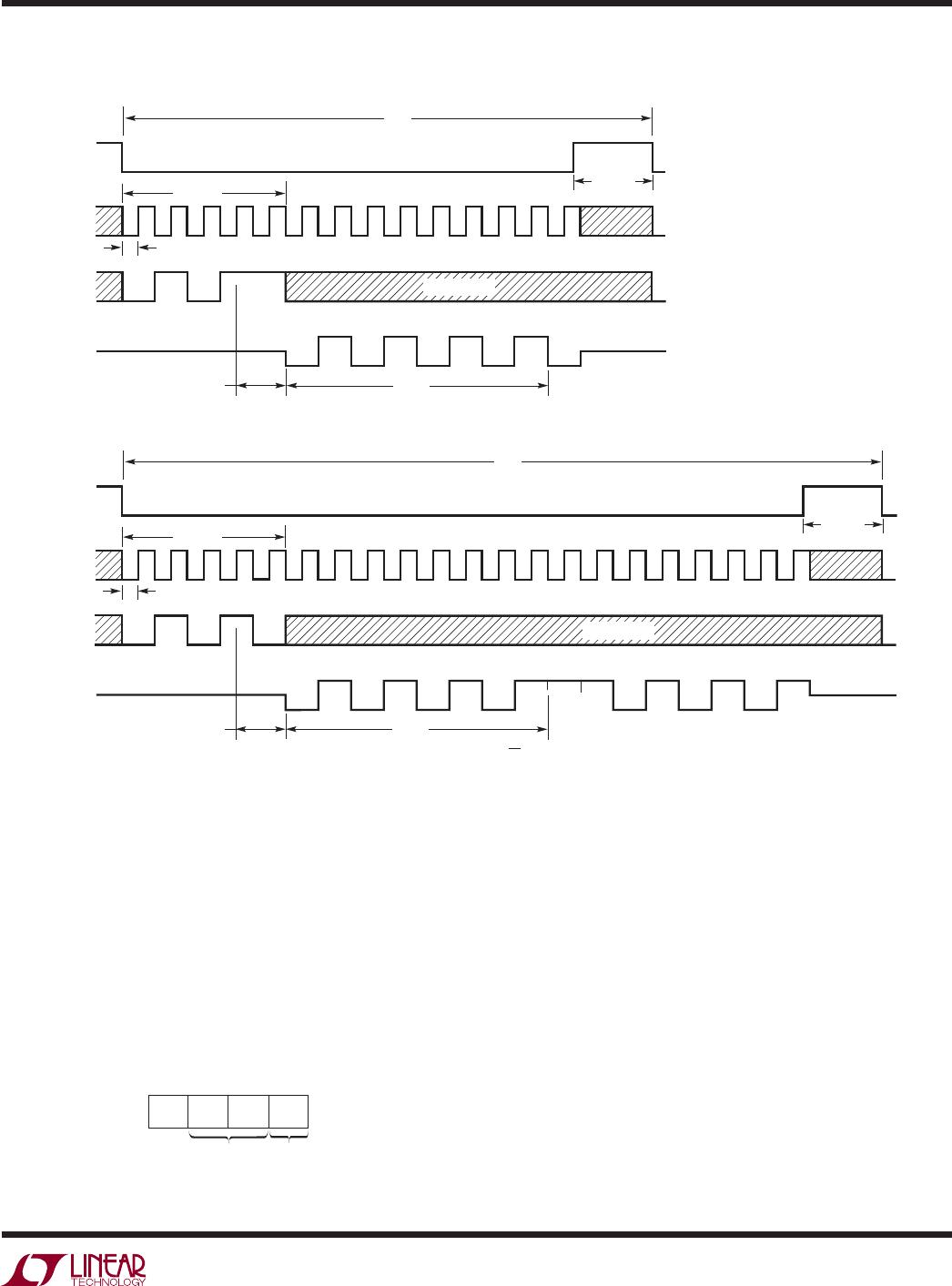
Data transfer is initiated by a falling chip select (CS) signal.
After CS falls the LTC1098(L) looks for a start bit. After the
start bit is received, the 3-bit input word is shifted into the
D
IN
input which confi gures the LTC1098(L) and starts the
conversion. After one null bit, the result of the conversion
Figure 1. LTC1096(L) Operating Sequence
is output on the D
OUT
line. At the end of the data exchange
CS should be brought high. This resets the LTC1098(L) in
preparation for the next data exchange.
The LTC1096(L) does not require a confi guration input
word and has no D
IN
pin. A falling CS initiates data trans-
feras shown in the LTC1096(L) operating sequence. After
CS falls, the fi rst CLK pulse enables D
OUT
. After one null
bit, the A/D conversion result is output on the D
OUT
line.
Bringing CS high resets the LTC1096(L) for the next data
exchange.
CLK
t
CYC
CS
B7*B6B5
B4
B3
B2B1
B0
B1
B2
B3B4B5
B6
B7
NULL
BIT
Hi-Z
D
OUT
10968 F01
POWER
DOWN
Hi-Z
t
suCS
t
WAKEUP
t
CONV
CLK
CS
t
CYC
POWER
DOWN
t
WAKEUP
B0
B1
B2
B3
B4B5
B6B7
Hi-Z
D
OUT
t
CONV
HI-Z
t
suCS
NULL
BIT
*AFTER COMPLETING THE DATA TRANSFER, IF FURTHER CLOCKS ARE APPLIED WITH CS LOW, THE ADC WILL OUTPUT ZEROS INDEFINITELY.
(MSB)
(MSB)
APPLICATIONS INFORMATION
D
IN
1 D
IN
2
D
OUT
1 D
OUT
2
CS
SHIFT MUX
ADDRESS IN
1 NULL BIT
SHIFT A/D CONVERSION
RESULT OUT
10968 AI01
LTC1096/LTC1096L
LTC1098/LTC1098L
17
10968fc
Input Data Word
The LTC1096(L) requires no D
IN
word. It is permanently
confi gured to have a single differential input. The conver-
sion result, in which output on the D
OUT
line is MSB-fi rst
sequence, followed by LSB sequence providing easy
interface to MSB- or LSB-fi rst serial ports.
The LTC1098(L) clocks data into the D
IN
input on the ris-
ing edge of the clock. The input data words are defi ned
as follows:
Start Bit
The fi rst “logical one” clocked into the D
IN
input after CS
goes low is the start bit. The start bit initiates the data
transfer. The LTC1098(L) will ignore all leading zeros which
precede this logical one. After the start bit is received,
the remaining bits of the input word will be clocked in.
Further inputs on the D
IN
pin are then ignored until the
next CS cycle.
APPLICATIONS INFORMATION
CLK
CS
t
CYC
POWER
DOWN
t
suCS
t
WAKEUP
D
IN
SGL/
DIFF
MSBF
B0*
B1
B2
B3
B4B5
B6B7
NULL
BIT
Hi-Z
D
OUT
t
CONV
t
SMPL
HI-Z
START
ODD/
SIGN
DON'T CARE
MSB-FIRST DATA (MSBF = 0)
MSB-FIRST DATA (MSBF = 1)
10968 F02
CLK
CS
t
CYC
POWER
DOWN
t
suCS
t
WAKEUP
D
IN
SGL/
DIFF
MSBF
B0
B1B2
B3
B4B5
B6
B7
NULL
BIT
Hi-Z
D
OUT
t
CONV
t
SMPL
HI-Z
START
ODD/
SIGN
DON'T CARE
B7*B6B5
B4
B3B2B1
*AFTER COMPLETING THE DATA TRANSFER, IF FURTHER CLOCKS ARE APPLIED WITH CS LOW, THE ADC WILL OUTPUT ZEROS INDEFINITELY.
(MSB)
(MSB)
Figure 2. LTC1098(L) Operating Sequence Example: Differential Inputs (CH
+
, CH
)
SGL/
DIFF
ODD/
SIGN
MSBFSTART
MUX
ADDRESS
MSB-FIRST
/
LSB-FIRST
10968 AI02
LTC1096/LTC1096L
LTC1098/LTC1098L
18
10968fc
APPLICATIONS INFORMATION
Multiplexer (MUX) Address
The bits of the input word following the START bit assign
the MUX confi guration for the requested conversion. For
a given channel selection, the converter will measure the
voltage between the two channels indicated by the “+”
and “–” signs in the selected row of the followintg tables.
In single-ended mode, all input channels are measured
with respect to GND.
MSB-First/LSB-First (MSBF)
The output data of the LTC1098(L) is programmed for
MSB-fi rst or LSB-fi rst sequence using the MSBF bit.
When the MSBF bit is a logical one, data will appear on
the D
OUT
line in MSB-fi rst format. Logical zeros will be
lled in indefi nitely following the last data bit. When the
MSBF bit is a logical zero, LSB-fi rst data will follow the
normal MSB-fi rst data on the D
OUT
line. (see Operating
Sequence)
MUX ADDRESS
SGL/DIFF
1
1
0
0
ODD/SIGN
0
1
0
1
CHANNEL #
0
+
+
1
+
+
GND
SINGLE-ENDED MUX MODE
DIFFERENTIAL MUX MODE
10968 AI03
OUTPUT CODE
1 1 1 1 1 1 1 1
1 1 1 1 1 1 1 0
0 0 0 0 0 0 0 1
0 0 0 0 0 0 0 0
INPUT VOLTAGE
V
REF
– 1LSB
V
REF
– 2LSB
1LSB
0V
INPUT VOLTAGE
(V
REF
= 5.000V)
4.9805V
4.9609V
0.0195V
0V
10968 AI05
0V
1LSB
V
REF
–2LSB
V
REF
–1LSB
V
REF
V
IN
0 0 0 0 0 0 0 1
0 0 0 0 0 0 0 0
1 1 1 1 1 1 1 1
1 1 1 1 1 1 1 0
10968 AI04
Unipolar Transfer Curve
The LTC1096(L)/LTC1098(L) are permanently confi gured
for unipolar only. The input span and code assignment for
this conversion type are shown in the following fi gures
for a 5V reference.
Unipolar Transfer Curve
LTC1098(L) Channel Selection
Unipolar Output Code
Operation with D
IN
and D
OUT
Tied Together
The LTC1098(L) can be operated with D
IN
and D
OUT
tied
together. This eliminates one of the lines required to com-
municate to the microprocessor (MPU). Data is transmit-
ted in both directions on a single wire. The processor pin
connected to this data line should be confi gurable as either
an input or an output. The LTC1098(L) will take control of

LTC1096LIS8#PBF

Mfr. #:
Manufacturer:
Analog Devices / Linear Technology
Description:
Analog to Digital Converters - ADC uP Smpl 8-B Serial I/O A/D Convs
Lifecycle:
New from this manufacturer.
Delivery:
DHL FedEx Ups TNT EMS
Payment:
T/T Paypal Visa MoneyGram Western Union