IRU1015-33
2
Rev. 1.2
08/01/02
www.irf.com
ABSOLUTE MAXIMUM RATINGS
Input Voltage (VIN) .................................................... 7V
Power Dissipation ..................................................... Internally Limited
Storage Temperature Range ...................................... -65°C To 150°C
Operating Junction Temperature Range ..................... 0°C To 150°C
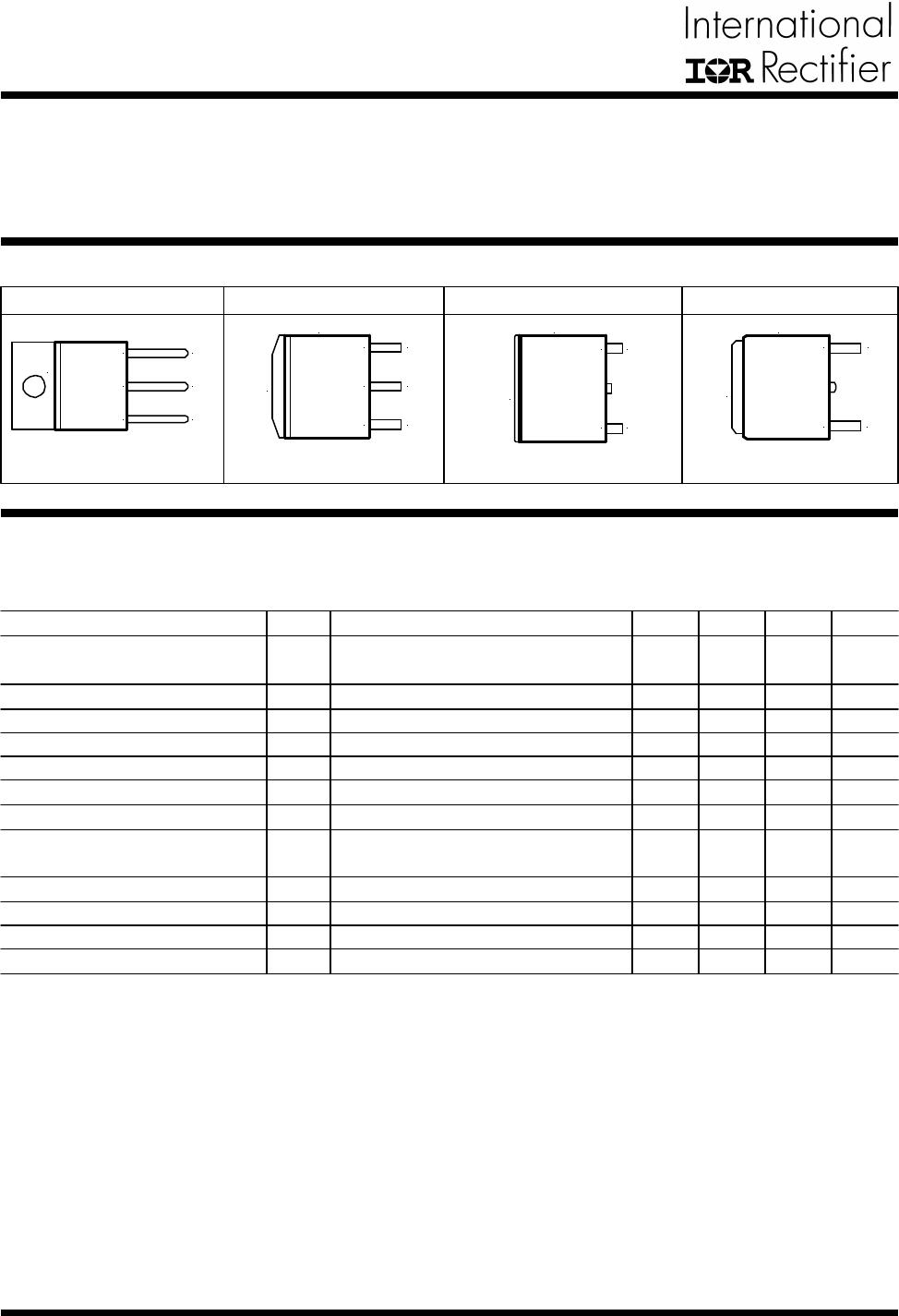
PACKAGE INFORMATION
3-PIN PLASTIC TO-220 (T) 3-PIN PLASTIC TO-263 (M) 2-PIN PLASTIC ULTRA THIN-PAK
TM
(P) 2-PIN PLASTIC TO-252 (D-Pak)
θJT=2.7°C/W θJA=60°C/W θJA=35°C/W for 1" Square pad θJA=70°C/W for 1" Square pad θJA=70°C/W for 0.5" Sq pad
Unless otherwise specified, these specifications apply over CIN=1µF, COUT=10µF, and TJ=0 to 1508C.
Typical values refer to TJ=258C.
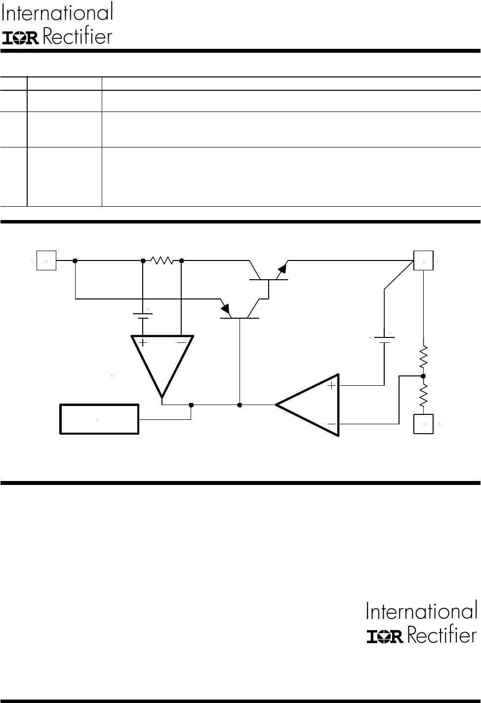
ELECTRICAL SPECIFICATIONS
Note 1: Low duty cycle pulse testing with Kelvin con-
nections is required in order to maintain accurate data.
Note 2: Dropout voltage is defined as the minimum dif-
ferential voltage between VIN and VOUT required to main-
tain regulation at VOUT. It is measured when the output
voltage drops 1% below its nominal value.
Note 3: Minimum load current is defined as the mini-
mum current required at the output in order for the out-
put voltage to maintain regulation. Typically the resistor
dividers are selected such that this current is automati-
cally maintained.
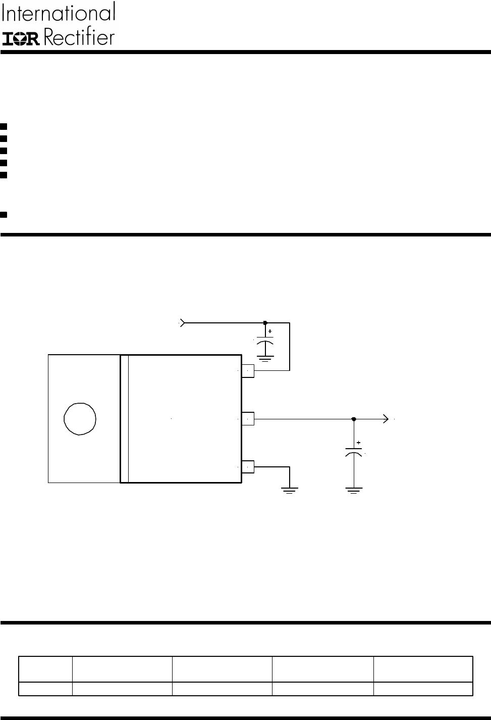
Gnd
VIN
VOUT
1
2
3
FRONT VIEW
Tab is
VOUT
Gnd
VOUT
VIN
Tab is
VOUT
FRONT VIEW
1
2
3
Gnd
V
IN
FRONT VIEW
1
3
Tab is
V
OUT
Gnd
VIN
1
3
FRONT VIEW
Tab is
VOUT
Io=10mA, TJ=258C, VIN=5V
Io=10mA, VIN=5V
Io=10mA, 4.7V<VIN<7V
VIN=5V, VADJ=0, 10mA<Io<1.5A
Note 2, Io=1.5A
VIN=5V, DVo=100mV
VIN=5V
30ms Pulse, VIN-Vo=3V, Io=1.5A
f=120Hz, Co=25mF Tantalum,
Io=0.75A, VIN-Vo=3V
Io=10mA, VIN-Vo=1.5V, TJ=258C
VIN=5V, VADJ=0V, Io=10mA
TJ=1258C, 1000Hrs
TJ=258C, 10Hz<f<10KHz
PARAMETER SYM TEST CONDITION MIN TYP MAX UNITS
Output Voltage
Line Regulation
Load Regulation (Note 1)
Dropout Voltage (Note 2)
Current Limit
Minimum Load Current (Note 3)
Thermal Regulation
Ripple Rejection
Adjust Pin Current Change
Temperature Stability
Long Term Stability
RMS Output Noise
Vo
DVo
3.267
3.234
1.6
60
3.300
3.300
1.1
5
0.01
70
0.2
0.5
0.3
0.003
3.333
3.366
0.2
0.4
1.3
10
0.02
5
1
V
%
%
V
A
mA
%/W
dB
mA
%
%
%Vo