DATASHEET
LVPECL Dual-Frequency
Programmable VCXO
IDT8N3DV85
IDT8N3DV85CCD REVISION A OCTOBER 30, 2013 1 ©2013 Integrated Device Technology, Inc.
General Description
The IDT8N3DV85 is a LVPECL Dual-Frequency Programmable
VCXO with very flexible frequency and pull-range programming
capabilities. The device uses IDT’s fourth generation FemtoClock
®
NG technology for an optimum of high clock frequency and low
phase noise performance. The device accepts 2.5V or 3.3V supply
and is packaged in a small, lead-free (RoHS 6) 6-lead ceramic 5mm
x 7mm x 1.55mm package.
The device can be factory-programmed to any two frequencies in the
range of 15.476MHz to 866.67MHz and from 975MHz to 1,300MHz
to the very high degree of frequency precision of 218Hz or better.
The output frequency is selected by the FSEL pin. The extended
temperature range supports wireless infrastructure, telecommuni-
cation and networking end equipment requirements.
Features
• Fourth Generation FemtoClock
®
NG technology
• Programmable clock output frequency from 15.476MHz to
866.67MHz and from 975MHz to 1,300MHz
• Two factory-programmed output frequencies
• VCO frequency programming resolution is 218Hz and better
• Factory-programmable VCXO pull range and control voltage
polarity
• VCXO pull range programmable from typical ±12.5 to ±787.5ppm
• One 2.5V or 3.3V LVPECL clock output
• FSEL control input for frequency selection, LVCMOS/LVTTL
compatible
• RMS phase jitter @ 622.08MHz (12kHz - 20MHz):0.46ps (typical)
• RMS phase jitter @ 622.08MHz (50kHz - 80MHz): 0.47ps (typical)
• 2.5V or 3.3V supply voltage
• -40°C to 85°C ambient operating temperature
• Lead-free (RoHS 6) 6-lead ceramic 5mm x 7mm x 1.55mm
package
1
2
3
6
5
4
VC
FSEL
V
EE
V
CC
nQ
Q
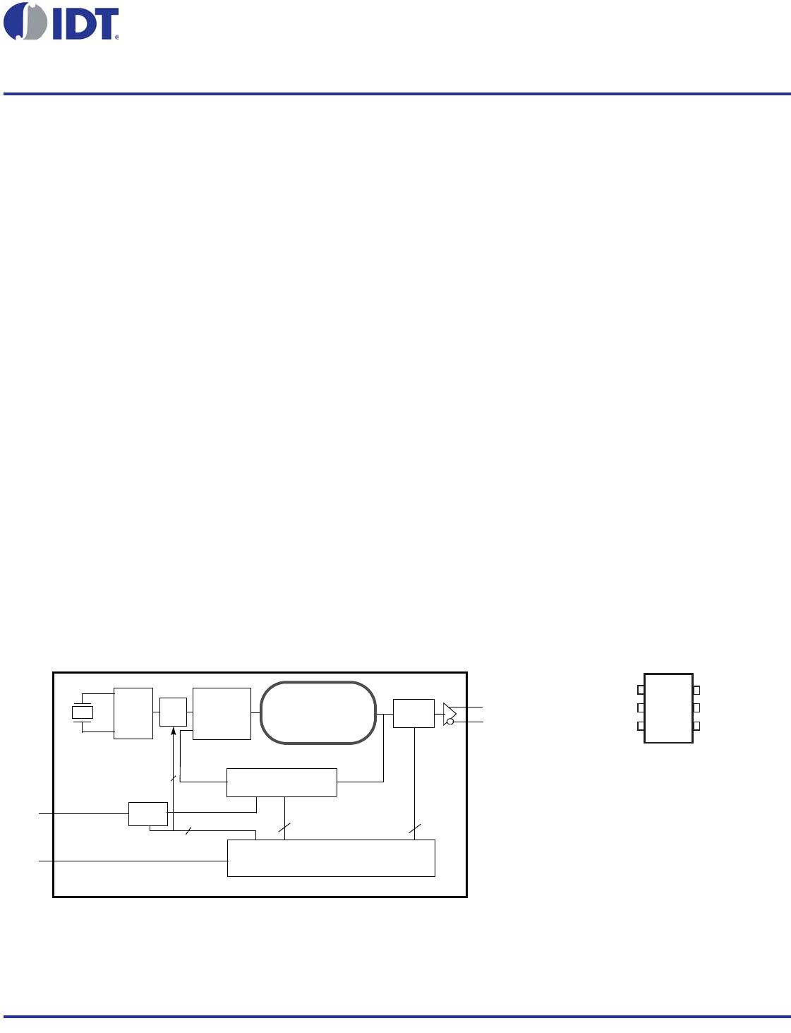
Block Diagram
Pin Assignment
IDT8N3DV85
6-lead ceramic 5mm x 7mm x 1.55mm
package body
CD Package
Top View
Q
nQ
OSC
114.285 MHz
÷MINT, MFRAC
PFD
&
LPF
FemtoClock
®
NG
VCO
1950-2600MHz
÷N
Configuration Register (ROM)
(Frequency, Pull range, Polarity)
23
7
VC
FSEL
Pulldown
A/D
9
÷P
2