LOW SKEW, 1-TO-16
DIFFERENTIAL-TO-LVDS CLOCK DISTRIBUTION CHIP
8516 DATA SHEET
4 REVISION B 6/11/15
TABLE 4A. POWER SUPPLY DC CHARACTERISTICS, V
DD
= 3.3V±5%, TA = 0°C TO 70°C
TABLE 4C. DIFFERENTIAL DC CHARACTERISTICS, V
DD
= 3.3V±5%, TA = 0°C TO 70°C
TABLE 4B. LVCMOS/LVTTL DC CHARACTERISTICS, V
DD
= 3.3V±5%, TA = 0°C TO 70°C
Symbol Parameter Test Conditions Minimum Typical Maximum Units
V
DD
Positive Supply Voltage 3.135 3.3 3.465 V
I
DD
Static Power Supply Current
RL = 100Ω
135 165 mA
No Load 60 75 mA
Symbol Parameter Test Conditions Minimum Typical Maximum Units
I
IH
Input High Current
CLK V
IN
= V
DD
= 3.465V 150 µA
nCLK V
IN
= V
DD
= 3.465V 5 µA
I
IL
Input Low Current
CLK V
DD
= 3.465V, V
IN
= 0V -5 µA
nCLK V
DD
= 3.465V, V
IN
= 0V -150 µA
V
PP
Peak-to-Peak Voltage 0.15 1.3 V
V
CMR
Common Mode Input Voltage;
NOTE 1, 2
GND + 0.5 V
DD
- 0.85 V
NOTE 1: For single ended applications, the maximum input voltage for CLK, nCLK is V
DD
+ 0.3V.
NOTE 2: Common mode voltage is defi ned ast
V
IH
.
Symbol Parameter Test Conditions Minimum Typical Maximum Units
V
IH
Input High Voltage OE1, OE2 2 V
DD
+ 0.3 V
V
IL
Input Low Voltage OE1, OE2 -0.3 0.8 V
I
IH
Input High Current OE1, OE2 V
DD
= V
IN
= 3.465V 5 µA
I
IL
Input Low Current OE1, OE2 V
DD
= 3.465V, V
IN
= 0V -150 µA
ABSOLUTE MAXIMUM RATINGS
Supply Voltage, V
DD
4.6V
Inputs, V
I
-0.5V to V
DD
+ 0.5 V
Outputs, V
O
-0.5V to V
DD
+ 0.5V
Package Thermal Impedance, θ
JA
47.9°C/W (0 lfpm)
Storage Temperature, T
STG
-65°C to 150°C
NOTE: Stresses beyond those listed under Absolute
Maximum Ratings may cause permanent damage to the
device. These ratings are stress specifi cations only. Functional
operation of product at these conditions or any conditions
beyond those listed in the DC Characteristics or AC Charac-
teristics is not implied. Exposure to absolute maximum rating
conditions for extended periods may affect product reliability.
REVISION B 6/11/15
8516 DATA SHEET
5 LOW SKEW, 1-TO-16
DIFFERENTIAL-TO-LVDS CLOCK DISTRIBUTION CHIP
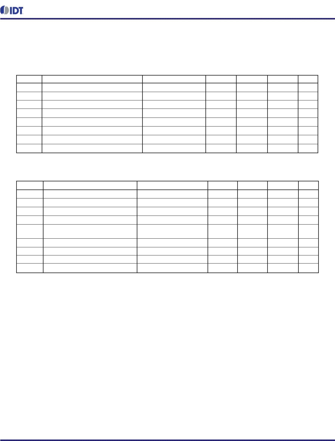
TABLE 5. AC CHARACTERISTICS, V
DD
= 3.3V±5%, TA = 0°C TO 70°C
TABLE 4D. LVDS DC CHARACTERISTICS, V
DD
= 3.3V±5%, TA = 0°C TO 70°C
Symbol Parameter Test Conditions Minimum Typical Maximum Units
V
OD
Differential Output Voltage 250 400 600 mV
Δ V
OD
V
OD
Magnitude Change 50 mV
V
OS
Offset Voltage 1.125 1.4 1.6 V
Δ V
OS
V
OS
Magnitude Change 50 mV
I
OZ
High Impedance Leakage Current -10 +10 µA
I
OFF
Power Off Leakage -1 +1 µA
I
OSD
Differential Output Short Circuit Current -5.5 mA
I
OS
/I
OSB
Output Short Circuit Current -12 mA
Symbol Parameter Test Conditions Minimum Typical Maximum Units
f
MAX
Output Frequency 700 MHz
t
PD
Propagation Delay; NOTE 1 1.6 2.0 2.4 ns
tsk(o) Output Skew; NOTE 2, 4 90 ps
tsk(pp) Part-to-Part Skew; NOTE 3, 4 500 ps
tjit
Buffer Additive Phase Jitter, RMS;
refer to Additive Phase Jitter Section
Integration Range:
12kHz - 20MHz
148 fs
t
R
/t
F
Output Rise/Fall Time 20% to 80% 100 550 ps
odc Output Duty Cycle 45 50 55 %
t
PZL
, t
PZH
Output Enable Time; NOTE 5 5 ns
t
PLZ
, t
PHZ
Output Disable Time; NOTE 5 5 ns
NOTE 1: Measured from the differential input crossing point to the differential output crossing point.
NOTE 2: Defi ned as skew between outputs at the same supply voltages and with equal load conditions.
Measured at the output differential cross points.
NOTE 3: Defi ned as skew between outputs on different devices operating at the same supply voltages
and with equal load conditions. Using the same type of inputs on each device, the outputs are measured
at the differential cross points.
NOTE 4: This parameter is defi ned in accordance with JEDEC Standard 65.
NOTE 5: These parameters are guaranteed by characterization. Not tested in production.
LOW SKEW, 1-TO-16
DIFFERENTIAL-TO-LVDS CLOCK DISTRIBUTION CHIP
8516 DATA SHEET
6 REVISION B 6/11/15
ADDITIVE PHASE JITTER
Additive Phase Jitter @ 155.52MHz
(12kHz to 20MHz)
= 148fs typical
-50
-60
-70
-80
-90
-100
-100
-120
-130
-140
-150
-160
1k 10k 100k 1M 10M 100M
The spectral purity in a band at a specifi c offset from the
fundamental compared to the power of the fundamental is
called the dBc Phase Noise. This value is normally expressed
using a Phase noise plot and is most often the specifi ed plot
in many applications. Phase noise is defi ned as the ratio of the
noise power present in a 1Hz band at a specifi ed offset from the
fundamental frequency to the power value of the fundamental.
This ratio is expressed in decibels (dBm) or a ratio of the power in
As with most timing specifi cations, phase noise measurements
have issues. The primary issue relates to the limitations of the
equipment. Often the noise fl oor of the equipment is higher
than the noise fl oor of the device. This is illustrated above. The
the 1Hz band to the power in the fundamental. When the required
offset is specifi ed, the phase noise is called a dBc value, which
simply means dBm at a specifi ed offset from the fundamental.
By investigating jitter in the frequency domain, we get a better
understanding of its effects on the desired application over the
entire time record of the signal. It is mathematically possible to
calculate an expected bit error rate given a phase noise plot.
device meets the noise fl oor of what is shown, but can actually
be lower. The phase noise is dependant on the input source and
measurement equipment.
OFFSET FROM CARRIER FREQUENCY (HZ)
SSB PHASE NOISE dBc/HZ

8516FYLF

Mfr. #:
Manufacturer:
IDT
Description:
Clock Buffer 1-to-16 LVDS Fanout Buffer
Lifecycle:
New from this manufacturer.
Delivery:
DHL FedEx Ups TNT EMS
Payment:
T/T Paypal Visa MoneyGram Western Union

Products related to this Datasheet