LTC3555/LTC3555-X
15
3555fe
For more information www.linear.com/LTC3555
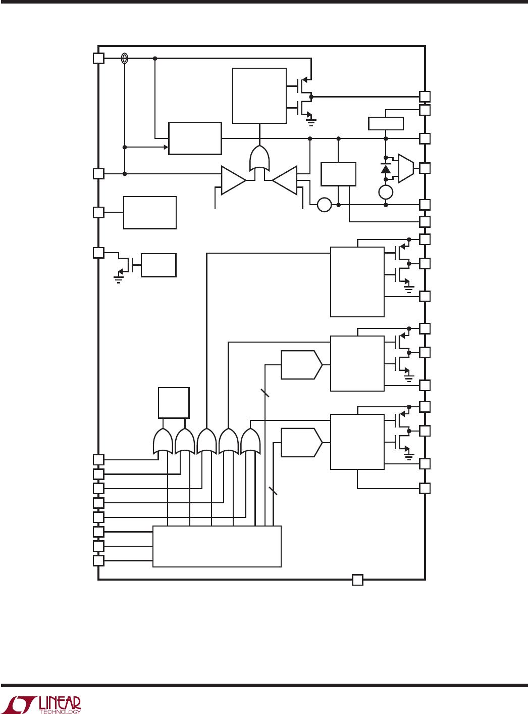
Introduction
The LTC3555 family are highly integrated power manage-
ment ICs which include a high efficiency switch mode
PowerPath controller, a battery charger, an ideal diode,
an always-on LDO and three general purpose step-down
switching regulators. The entire chip is controlled by either
direct digital control, by an I
2
C serial port or both.
Designed specifically for USB applications, the PowerPath
controller incorporates a precision average input current
step-down switching regulator to make maximum use of
the allowable USB power. Because power is conserved, the
LTC3555 family allows the load current on V
OUT
to exceed
the current drawn by the USB port without exceeding the
USB load specifications.
The PowerPath switching regulator and battery charger
communicate to ensure that the input current never violates
the USB specifications.
The ideal diode from BAT to V
OUT
guarantees that ample
power is always available to V
OUT
even if there is insuf-
ficient or absent power at V
BUS
.
An “always on” LDO provides a regulated 3.3V from
available power at V
OUT
. Drawing very little quiescent
current, this LDO will be on at all times and can be used
to supply up to 25mA.
The three general purpose switching regulators can be
independently enabled via either direct digital control or
by operating the I
2
C serial port. Under I
2
C control, two of
the three switching regulators have adjustable set-points
so that voltages can be reduced when high processor
performance is not needed. Along with constant frequency
PWM mode, all three switching regulators have a low
power burst-only mode setting as well as automatic Burst
Mode operation and LDO modes for significantly reduced
quiescent current under light load conditions.
High Efficiency Switching PowerPath Controller
Whenever V
BUS
is available and the PowerPath switching
regulator is enabled, power is delivered from V
BUS
to V
OUT
via SW. V
OUT
drives the combination of the external load
(switching regulators 1, 2 and 3) and the battery charger.
If the combined load does not exceed the PowerPath switch-
ing regulator’s programmed input current limit, V
OUT
will
track 0.3V above the battery. By keeping the voltage across
the battery charger low, efficiency is optimized because
power lost to the linear battery charger is minimized.
Power available to the external load is therefore optimized.
OPERATION