H11A1-X009T

H11A1, H11A2, H11A3, H11A4, H11A5
www.vishay.com
Vishay Semiconductors
End of Life January-2018 - Alternative Device: CNY17
Rev. 1.7, 23-Jul-15
1
Document Number: 83730
For technical questions, contact: optocoupleranswers@vishay.com
THIS DOCUMENT IS SUBJECT TO CHANGE WITHOUT NOTICE. THE PRODUCTS DESCRIBED HEREIN AND THIS DOCUMENT
ARE SUBJECT TO SPECIFIC DISCLAIMERS, SET FORTH AT www.vishay.com/doc?91000
Optocoupler, Phototransistor Output, with Base Connection
DESCRIPTION
The H11Ax family is an industry standard single channel
phototransistor coupler. It includes the H11A1, H11A2,
H11A3, H11A4, H11A5 couplers.
Each optocoupler consists of gallium arsenide infrared LED
and a silicon NPN phototransistor.
The isolation performance is accomplished through Vishay
double molding isolation manufacturing process.
Compliance to DIN EN 60747-5-5 partial discharge isolation
specification is available is by ordering option 1.
These isolation processes and the Vishay ISO9001 quality
program results in the highest isolation performance
available for a commercial plastic phototransistor
optocoupler.
The devices are available in lead formed configuration
suitable for surface mounting and are available either on
tape and reel, or in standard tube shipping containers.
Note
Designing with data sheet is covered in Application Note 45.
FEATURES
Interfaces with common logic families
Input-output coupling capacitance < 0.5 pF
Industry standard dual-in line 6-pin package
Isolation rated voltage 4420 V
RMS
Material categorization:
for definitions of compliance please see
www.vishay.com/doc?99912
APPLICATIONS
AC mains detection
Reed relay driving
Switch mode power supply feedback
Telephone ring detection
Logic ground isolation
Logic coupling with high frequency noise rejection
AGENCY APPROVALS
UL1577, file no. E52744, double protection
cUL tested to CSA 22.2 bulletin 5A
CSA 93751
BSI EN 60950, BSI EN 60065
DIN EN 60747-5-5 (VDE 0884-5), available with option 1
•FIMKO
CQC: GB 8898-2011, GB 4943.1-2011
Note
Additional options may be possible, please contact sales office.
3
B
C
E
A
C
NC
1
2
6
5
4
i179004-3
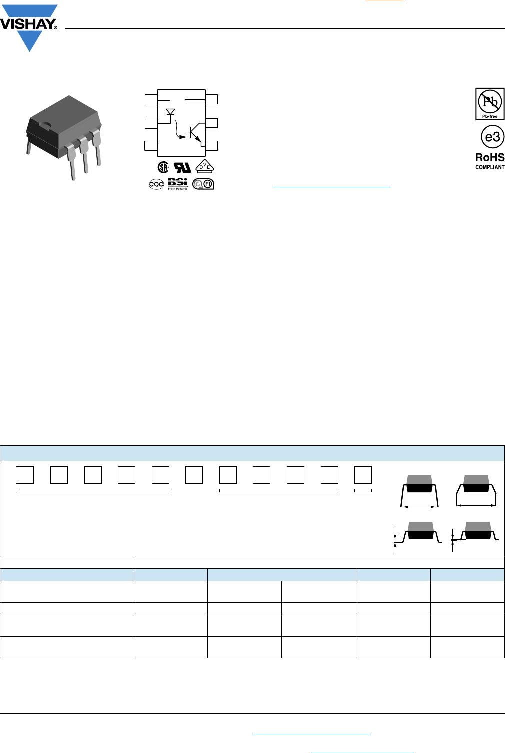
ORDERING INFORMATION
H11A#-X00#X
PART NUMBER PACKAGE OPTION TAPE
AND
REEL
AGENCY CERTIFIED/PACKAGE CTR (%)
UL, CSA, BSI, FIMKO, CQC > 50 > 20 > 10 > 30
DIP-6
H11A1,
H11A1-X001
H11A2 H11A3 H11A4 H11A5
DIP-6, 400 mil, option 6 H11A1-X006 - - - -
SMD-6, option 7
H11A1-X007,
H11A1-X017
----
SMD-6, option 9
H11A1-X009,
H11A1-X009T
----
> 0.1 mm
10.16 mm
> 0.7 mm
7.62 mm
DIP
Option 7
Option 6
Option 9
H11A1, H11A2, H11A3, H11A4, H11A5
www.vishay.com
Vishay Semiconductors
End of Life January-2018 - Alternative Device: CNY17
Rev. 1.7, 23-Jul-15
2
Document Number: 83730
For technical questions, contact: optocoupleranswers@vishay.com
THIS DOCUMENT IS SUBJECT TO CHANGE WITHOUT NOTICE. THE PRODUCTS DESCRIBED HEREIN AND THIS DOCUMENT
ARE SUBJECT TO SPECIFIC DISCLAIMERS, SET FORTH AT www.vishay.com/doc?91000
Note
Stresses in excess of the absolute maximum ratings can cause permanent damage to the device. Functional operation of the device is not
implied at these or any other conditions in excess of those given in the operational sections of this document. Exposure to absolute
maximum ratings for extended periods of the time can adversely affect reliability.
Note
Minimum and maximum values were tested requirements. Typical values are characteristics of the device and are the result of engineering
evaluations. Typical values are for information only and are not part of the testing requirements.
ABSOLUTE MAXIMUM RATINGS (T
amb
= 25 °C, unless otherwise specified)
PARAMETER TEST CONDITION SYMBOL VALUE UNIT
INPUT
Reverse voltage V
R
6V
Forward current I
F
60 mA
Surge current t 10 μs I
FSM
2.5 A
Power dissipation P
diss
100 mW
OUTPUT
Collector emitter breakdown voltage V
CEO
70 V
Emitter base breakdown voltage V
EBO
7V
Collector current
I
C
50 mA
t < 1 ms I
C
100 mA
Power dissipation P
diss
150 mW
COUPLER
Storage temperature range T
stg
-55 to +150 °C
Operating temperature range T
amb
-55 to +100 °C
Junction temperature T
j
100 °C
Soldering temperature
Max. 10 s, dip soldering: distance
to seating plane 1.5 mm
T
sld
260 °C
ELECTRICAL CHARACTERISTICS (T
amb
= 25 °C, unless otherwise specified)
PARAMETER TEST CONDITION PART SYMBOL MIN. TYP. MAX. UNIT
INPUT
Forward voltage I
F
= 10 mA
H11A1 V
F
1.1 1.5 V
H11A2 V
F
1.1 1.5 V
H11A3 V
F
1.1 1.5 V
H11A4 V
F
1.1 1.5 V
H11A5 V
F
1.1 1.7 V
Reverse current V
R
= 3 V I
R
10 μA
Capacitance V
R
= 0 V, f = 1 MHz C
O
50 pF
OUTPUT
Collector emitter breakdown voltage I
C
= 1 mA, I
F
= 0 mA BV
CEO
30 V
Emitter collector breakdown voltage I
E
= 100 μA, I
F
= 0 mA BV
ECO
7V
Collector base breakdown voltage I
C
= 10 μA, I
F
= 0 mA BV
CBO
70 V
Collector emitter leakage current V
CE
= 10 V, I
F
= 0 mA I
CEO
550nA
Emitter collector capacitance V
CE
= 0 V C
CE
6pF
COUPLER
Collector emitter, saturation voltage I
CE
= 0.5 mA, I
F
= 10 mA V
CEsat
0.4 V
Capacitance (input-output) C
IO
0.5 pF
CURRENT TRANSFER RATIO
PARAMETER TEST CONDITION PART SYMBOL MIN. TYP. MAX. UNIT
I
C
/I
F
V
CE
= 10 V, I
F
= 10 mA
H11A1 CTR
DC
50 %
H11A2 CTR
DC
20 %
H11A3 CTR
DC
20 %
H11A4 CTR
DC
10 %
H11A5 CTR
DC
30 %
H11A1, H11A2, H11A3, H11A4, H11A5
www.vishay.com
Vishay Semiconductors
End of Life January-2018 - Alternative Device: CNY17
Rev. 1.7, 23-Jul-15
3
Document Number: 83730
For technical questions, contact: optocoupleranswers@vishay.com
THIS DOCUMENT IS SUBJECT TO CHANGE WITHOUT NOTICE. THE PRODUCTS DESCRIBED HEREIN AND THIS DOCUMENT
ARE SUBJECT TO SPECIFIC DISCLAIMERS, SET FORTH AT www.vishay.com/doc?91000
Note
As per IEC 60747-5-5, § 7.4.3.8.2, this optocoupler is suitable for “safe electrical insulation” only within the safety ratings. Compliance with
the safety ratings shall be ensured by means of protective circuits.
TYPICAL CHARACTERISTICS (T
amb
= 25 °C, unless otherwise specified)
Fig. 1 - Forward Voltage vs. Forward Current Fig. 2 - Normalized Non-Saturated and Saturated CTR vs.
LED Current
SWITCHING CHARACTERISTICS
PARAMETER TEST CONDITION SYMBOL MIN. TYP. MAX. UNIT
Turn-on time
I
C
= 2 mA, R
L
= 100 Ω, V
CE
= 10 V
t
on
s
Turn-off time t
off
s
SAFETY AND INSULATION RATINGS
PARAMETER TEST CONDITION SYMBOL VALUE UNIT
Climatic classification According to IEC 68 part 1 55/100/21
Comparative tracking index CTI 175
Maximum rated withstanding isolation voltage t = 1 min V
ISO
4420 V
RMS
Maximum transient isolation voltage V
IOTM
10 000 V
peak
Maximum repetitive peak isolation voltage V
IORM
890 V
peak
Isolation resistance
V
IO
= 500 V, T
amb
= 25 °C R
IO
10
12
Ω
V
IO
= 500 V, T
amb
= 100 °C R
IO
10
11
Ω
Output safety power P
SO
400 mW
Input safety current I
SI
275 mA
Safety temperature T
S
175 °C
Creepage distance 7mm
Clearance distance 7mm
Insulation thickness DTI 0.4 mm
i4n25_01
1001010.1
0.7
0.8
0.9
1.0
1.1
1.2
1.3
1.4
I
F
- Forward Current (mA)
V
F
-Forward Voltage (V)
T
A
= - 55 °C
T
A
= 25 °C
T
A
= 85 °C
i4n25_02
0.0
0.5
1.0
1.5
0 10 100
I
F
- LED Current (mA)
NCTR
NCTR(SAT)
NCTR - Normalized CTR
CTR
CE(sat)
= 0.4 V
V
CE
= 10 V, I
F
= 10 mA, T
A
= 25 °C
T
A
= 25 °C
Normalized to:
1

H11A1-X009T

Mfr. #:
Manufacturer:
Vishay Semiconductors
Description:
Transistor Output Optocouplers Optocoupler SMD6
Lifecycle:
New from this manufacturer.
Delivery:
DHL FedEx Ups TNT EMS
Payment:
T/T Paypal Visa MoneyGram Western Union