6/13
XC6120 Series
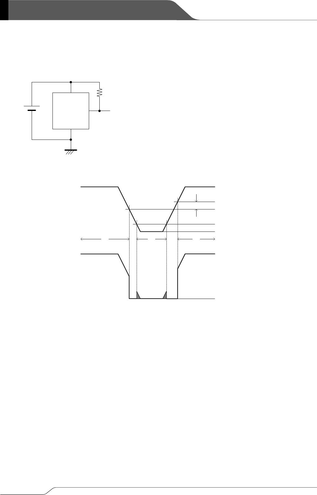
■OPERATIONAL EXPLANATION
The following explains the operation of the typical application circuit along number symbols shown in the timing chart.
① When input voltage (V
IN
) is higher than detect voltage (V
DF
), output voltage (V
OUT
) will be equal to input voltage (V
IN
).
(A condition of high impedance exists with N-ch open drain output configurations.)
② When input voltage (V
IN
) falls below detect voltage (V
DF
), output voltage (V
OUT
) will be equal to the ground voltage
(V
SS
) level.
③ When input voltage (V
IN
) falls to a level below that of the minimum operating voltage (V
MIN
), output will become
unstable. If In this condition, V
IN
will equal the pulled-up output (should output be pulled-up.) (Input voltage, V
IN
, in
the typical application circuit.)
④ When input voltage (V
IN
) rises above the minimum operating voltage (V
MIN
) level until it achieves a release voltage
(V
DR
), output keeps the ground voltage level (V
SS
).
⑤ When the input voltage (V
IN
) rises above the release voltage (V
DR
), output voltage (V
OUT
will be equal to input voltage
(V
IN
). (A condition of high impedance exists with N-ch open drain output configurations.)
⑥ The difference between V
DR
and V
DF
represents the hysteresis width.
●Timing Charge
●Typical Application Circuit
Note: For explaining in a simplified case, an operation time of the circuit is not counted.
VIN
VSS
VOUT
VIN
VOUT
R
PULL
(Unused for the CMOS output products)
Input Voltage
(V
IN
)
Output
Voltage
(V
OUT
)
Release Voltage (V
DR
)
Detect Voltage (V
DF
)
Minimum Operating Voltage (V
MIN
)
Ground Voltage (V
SS
)
Ground Voltage (V
SS
)
①② ④③ ⑤
⑥

