7/13
XC6120
Series
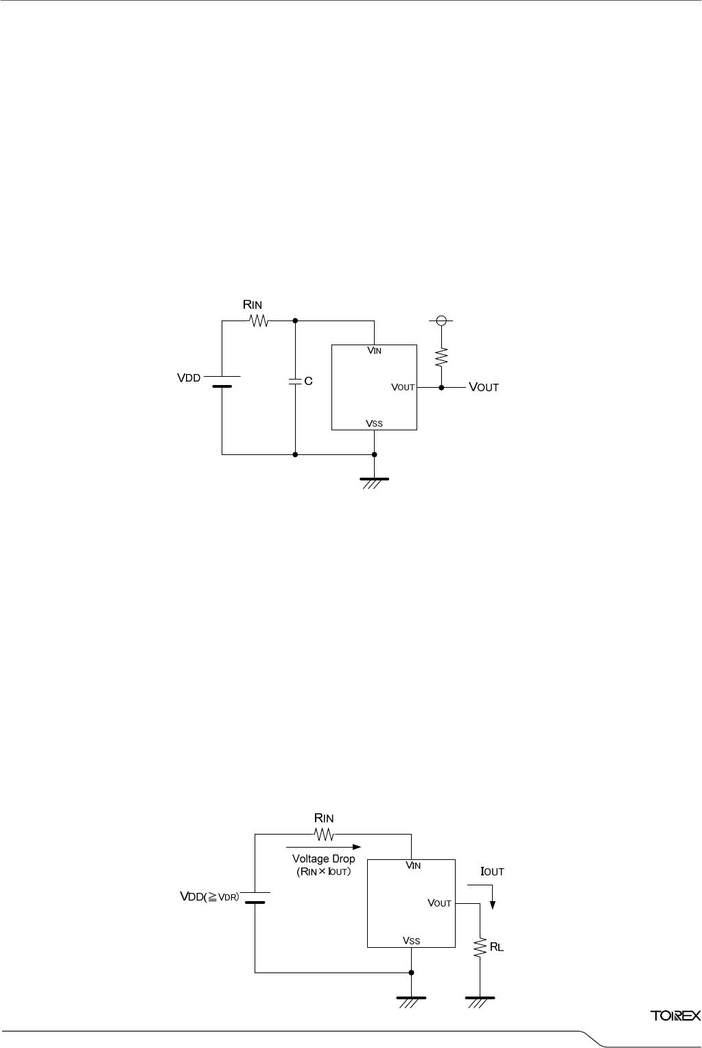
[Figure 1: Circuit connected with the input resistor]
● Oscillation Description
[Figure 2: Oscillation caused by the input resistor of the CMOS output product and the output current]
■NOTE ON USE
1. Please use this IC within the stated maximum ratings. For temporary, transitional voltage drop or voltage rising
phenomenon, the IC is liable to malfunction should the ratings be exceeded.
2. In order to stabilize the IC's operations, please ensure that V
IN
pin's input frequency's rise and fall times are more than
several μs / V.
3. With a resistor connected between the V
IN
pin and the power supply V
DD
some errors may be observed from the input
voltage at the detect and release voltage. Those errors are not constant because of the fluctuation of the supply current.
4. When a resistor is connected between the V
IN
pin and the power supply V
DD
, oscillation may occur as a result of through
current and voltage drop at the R
IN
at the time of voltage release. (refer to the Oscillation Description (1) below ) Especially
in the CMOS output configurations, oscillation may occur regardless of detect/release operation if load current (I
OUT
)
exists. (refer to the Oscillation Description (2) below)
5. Please use N-ch open drains configuration, when a resistor R
IN
is connected between the V
IN
pin and the power supply
V
DD
power source. In such cases, please ensure that R
IN
is less than 10kΩ and that C is more than 0.1μF.
6. Torex places an importance on improving our products and its reliability.
However, by any possibility, we would request user fail-safe design and post-aging treatment on system or equipment.
(1) Oscillation as a result of through current
Since the XC6120 series are CMOS ICs, transient through current will flow when the IC's internal circuit switching operates
regardless of output configuration. Consequently, oscillation is liable to occur as a result of the similar operations as in (1)
above. This oscillation does not occur during the detect operation.
(2) Output current oscillation with the CMOS output configuration
As shown in figure 2, when the voltage applied at the power supply (V
DD
) rises from below detect voltage to above release
voltage, the IC commence release operations and the internal P-ch driver transistor will be on. The output current (I
OUT
) flows
the input resistor (R
IN
) via the P-ch driver transistor. Because of the input resistor (R
IN
) and the output current (I
OUT
), an input pin
voltage drops R
IN
x I
OUT
. If the voltage drop level is larger than the IC’s hysteresis width (V
HYS
), the input pin voltage will falls
below the V
DF
and detect operations will commerce so that the internal P-ch driver transistor will be off. The voltage drop will
stop because the output current (I
OUT
) which was flowing the P-ch driver transistor will run down. The input pin voltage will
become the same voltage level as the input voltage (V
IN
). For this, the input pin voltage will rise above the release voltage (V
DR
),
therefore, the release operations will begin over again. Oscillation may occur with this repetition. Further, this condition will
also appear via means of a similar mechanism during detect operations.
XC6120N
XC6120C
V
PULL
R
PULL