4© 2008 Semtech Corp.
www.semtech.com
PRELIMINARY
PROTECTION PRODUCTS
EClamp2376K
Device Connection
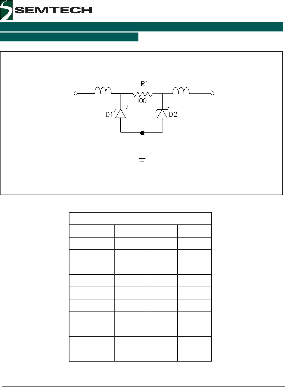
The EClamp2376K is comprised of six identical circuits
each consisting of a low pass filter for EMI/RFI sup-
pression and dual TVS diodes for ESD protection. The
device is in a 12-pin SLP package. Electrical connec-
tion is made to the 12 pins located at the bottom of
the device. A center tab serves as the ground connec-
tion. The device has a flow through design for easy
layout. Pin connections are noted in Figure 1. All path
lengths should be kept as short as possible to minimize
the effects of parasitic inductance in the board traces.
Recommendations for the ground connection are given
below.
Ground Connection Recommendation
Parasitic inductance present in the board layout will
affect the filtering performance of the device. As
frequency increases, the effect of the inductance
becomes more dominant. This effect is given by
Equation 1.
Equation 1: The Impedance of an Inductor at
Frequency XLF
L*f**2)f,L(XLF π=
Where:
L= Inductance (H)
f = Frequency (Hz)
Via connections to the ground plane form rectangular
wire loops or ground loop inductance as shown in
Figure 2. Ground loop inductance can be reduced by
using multiple vias to make the connection to the
ground plane. Bringing the ground plane closer to the
signal layer (preferably the next layer) also reduces
ground loop inductance. Multiple vias in the device
ground pad will result in a lower inductive ground loop
over two exterior vias. Vias with a diameter d are
separated by a distance y run between layers sepa-
rated by a distance x. The inductance of the loop path
is given by Equation 2. Thus, decreasing distance x
and y will reduce the loop inductance and result in
better high frequency filter characteristics.
niPnoitacifitnedI
6-1seniLtupnI
21-7seniLtuptuO
baTretneCdnuorG
Figure 2 - Inductance of Rectangular Wire Loops
Ground
Via 1
Signal Layer
Ground Layer
Layer
y
x
d
Ground
Via 2
Ground
Via 1
Signal Layer
Ground Layer
Layer
y
x
d
Ground
Via 2
[]
d
x*2
d
y*2
9
ln*yln*x*10*16.10)y,x,d(LRECT +=
−
Where:
d = Diameter of the wire (in)
x = Length of wire loop (in)
y = Breath of wire loop (in)
Equation 2: Inductance of Rectangular Wire Loop
Figure 1 - Pin Identification and Configuration
(Top Side View)
In 1
In 2
In 3
In 4
Out 1
Out 2
Out 3
Out 4
In 5
In 6
Out 5
Out 6
1
67
12
GND