Typical Operating Characteristics (continued)
(V
DD
= 2.7V, V
REF
= 2.5V
EXTERNAL
, f
DCLK
= 2MHz, f
SAMPLE
= 125kHz, C
LOAD
= 50pF, 0.1µF capacitor at REF, T
A
= +25°C, unless
otherwise noted.)
MXB7846
2.375V to 5.25V, 4-Wire Touch-Screen Controller
with Internal Reference and Temperature Sensor
_______________________________________________________________________________________
7
SUPPLY CURRENT
vs. SUPPLY VOLTAGE
MXB7846 toc18
SUPPLY VOLTAGE (V)
SUPPLY CURRENT (μA)
5.04.54.03.53.02.5
175
200
225
250
150
2.0 5.5
f
SAMPLE
= 12.5kHz
SUPPLY CURRENT vs. TEMPERATURE
MXB7846 toc19
TEMPERATURE (°C)
SUPPLY CURRENT (μA)
6550-25 -10 5 20 35
255
260
265
270
275
280
285
290
250
-40 80
f
SAMPLE
= 125kHz
V
DD
= 2.7V
SUPPLY CURRENT vs. SAMPLE RATE
MXB7846 toc20
SAMPLE RATE (kHz)
SUPPLY CURRENT (μA)
100755025
125
150
175
200
225
250
100
0 125
V
DD
= 2.7V
V
REF
= 2.5V
SHUTDOWN CURRENT
vs. SUPPLY VOLTAGE
MXB7846 toc21
SUPPLY VOLTAGE (V)
SHUTDOWN CURRENT (nA)
4.74.23.73.2
100
150
200
250
300
50
2.7 5.2
DCLK = CS = V
DD
SHUTDOWN CURRENT vs. TEMPERATURE
MXB7846 toc22
TEMPERATURE (°C)
SHUTDOWN CURRENT (nA)
655035205-10-25
60
70
80
90
100
110
120
50
-40 80
DCLK = CS = V
DD
= 3V
MAXIMUM SAMPLE RATE
vs. SUPPLY VOLTAGE
MXB7846 toc23
SUPPLY VOLTAGE (V)
SAMPLE RATE (kHz)
5.04.54.03.53.02.5
10
100
1000
1
2.0 5.5
Pin Description
MXB7846
2.375V to 5.25V, 4-Wire Touch-Screen Controller
with Internal Reference and Temperature Sensor
8 _______________________________________________________________________________________
CS
DCLK
DIN
DOUT
BUSY
t
BDV
t
DV
t
CSS
t
CL
t
CH
t
DS
t
DH
t
CP
t
DO
t
BD
t
TR
t
BTR
t
CSH
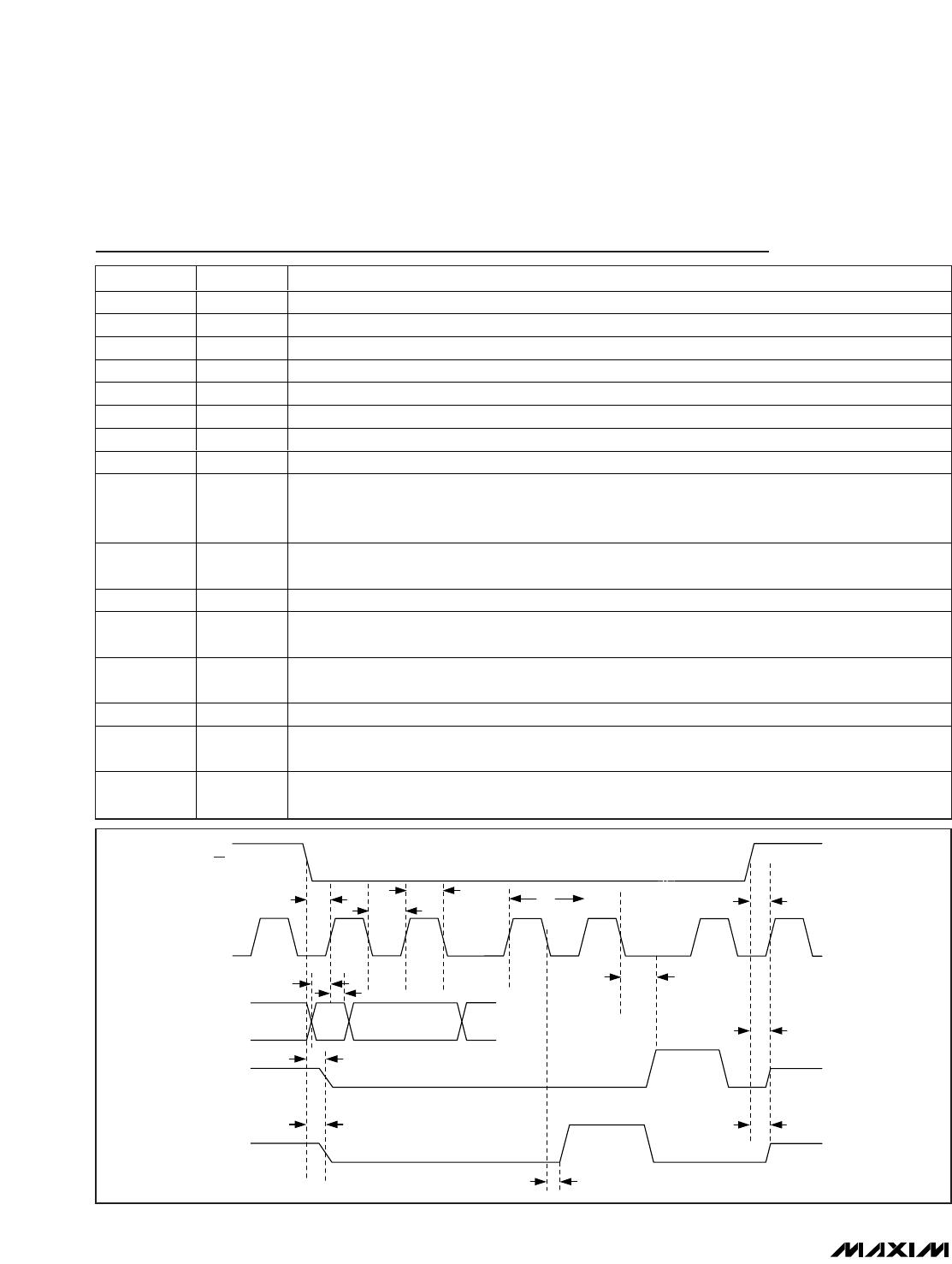
Figure 1. Detailed Serial Interface Timing
PIN NAME FUNCTION
1V
DD
Positive Supply Voltage. Connect to pin 10.
2 X+ X+ Position Input, ADC Input Channel 1
3 Y+ Y+ Position Input, ADC Input Channel 2
4 X- X- Position Input
5 Y- Y- Position Input
6 GND Ground
7 BAT Battery Monitoring Inputs; ADC Input Channel 3
8 AUX Auxiliary Input to ADC; ADC Input Channel 4
9 REF
Voltage Reference Output/Input. Reference voltage for analog-to-digital conversion. In internal
reference mode, the reference buffer provides a 2.50V nominal output. In external reference mode,
apply a reference voltage between 1V and V
DD
. Bypass REF to GND with a 0.1µF capacitor.
10 V
DD
Positive Supply Voltage, +2.375V (2.70V) to +5.25V. External (internal) reference. Bypass with a 1µF
capacitor. Connect to pin 1.
11 PENIRQ Pen Interrupt Output. Open anode output. 10kΩ to 100kΩ pullup resistor required to V
DD
.
12 DOUT
Serial Data Output. Data changes state on the falling edge of DCLK. High impedance when CS is
HIGH.
13 BUSY
Busy Output. BUSY pulses high for one clock period before the MSB decision. High impedance when
CS is HIGH.
14 DIN Serial Data Input. Data clocked in on the rising edge of DCLK.
15 CS
Active-Low Chip Select. Data is only clocked into DIN when CS is low. When CS is HIGH, DOUT and
BUSY are high impedance.
16 DCLK
Serial Clock Input. Clocks data in and out of the serial interface and sets the conversion speed (duty
cycle must be 40% to 60%).
MXB7846
2.375V to 5.25V, 4-Wire Touch-Screen Controller
with Internal Reference and Temperature Sensor
_______________________________________________________________________________________ 9
Detailed Description
The MXB7846 uses a successive-approximation conver-
sion technique to convert analog signals to a 12-bit digi-
tal output. An SPI/QSPI/MICROWIRE™-compatible serial
interface provides easy communication to a micro-
processor (µP). It features an internal 2.5V reference, an
on-chip temperature sensor, a battery monitor, and a
4-wire touch-screen interface (
Functional Diagram
).
Analog Inputs
Figure 2 shows a block diagram of the analog input sec-
tion that includes the input multiplexer of the MXB7846,
the differential signal inputs of the ADC, and the differ-
ential reference inputs of the ADC. The input multiplexer
switches between X+, X-, Y+, Y-, AUX, BAT, and the
internal temperature sensor.
In single-ended mode, conversions are performed using
REF as the reference. In differential mode, ratiometric
conversions are performed with REF+ connected to X+ or
Y+, and REF- connected to X- or Y-. Configure the refer-
ence and switching matrix according to Tables 1 and 2.
During the acquisition interval, the selected channel
charges the sampling capacitance. The acquisition
interval starts on the fifth falling clock edge and ends
on the eighth falling clock edge.
The time required for the T/H to acquire an input signal
is a function of how quickly its input capacitance is
charged. If the input signal’s source impedance is high,
the acquisition time lengthens, and more time must be
allowed between conversions. The acquisition time
(t
ACQ
) is the maximum time the device takes to acquire
the input signal to 12-bit accuracy. Calculate t
ACQ
with
the following equation:
where R
IN
= 2kΩ and R
S
is the source impedance of
the input signal.
Source impedances below 1kΩ do not significantly affect
the ADC’s performance. Accommodate higher source
impedances by either slowing down DCLK or by placing
a 1µF capacitor between the analog input and GND.
tRRpF
ACQ S IN
. +
()
×84 25
MICROWIRE is a trademark of National Semiconductor Corp.
+V
DD
PENIRQ
TEMP1
V
REF
A2–A0
(SHOWN 001
B
)
SER/DFR
(SHOWN HIGH)
GND
X+
X-
Y+
Y-
12-BIT ADC
AUX
V
BAT
REF+
REF-
REF ON/OFF
7.5kΩ
2.5kΩ
2.5V
REFERENCE
BATTERY
ON
+IN
-IN
TEMP0
MXB7846
Figure 2. Equivalent Input Circuit

MXB7846EEE+T

Mfr. #:
Manufacturer:
Maxim Integrated
Description:
Touch Screen Controllers 2.375-5.25V 4-Wire Touch-Screen Ctlr
Lifecycle:
New from this manufacturer.
Delivery:
DHL FedEx Ups TNT EMS
Payment:
T/T Paypal Visa MoneyGram Western Union

Products related to this Datasheet