APT1
–3–
ASCTB217E 201410-T
2) DIP4/6 type and DIP4/6 Wide terminal type
Note: “A”, “AX”, “AZ” “AY” and “AW” at the end of the part numbers have been omitted.
* Do not exceed 0.05 A of ON state RMS current in case of following load voltage condition.
DIP4pin (APT1211, APT1221, APT1231) and DIP4pin wide terminal type (APT1211W, APT1221W, APT1231W): more than 100 V AC;
DIP6pin (APT1212, APT1222, APT1232) and DIP6pin wide terminal type (APT1212W, APT1222W, APT1232W): more than 120 V AC.
2. Characteristics (Ambient temperature: 25°C 77°F)
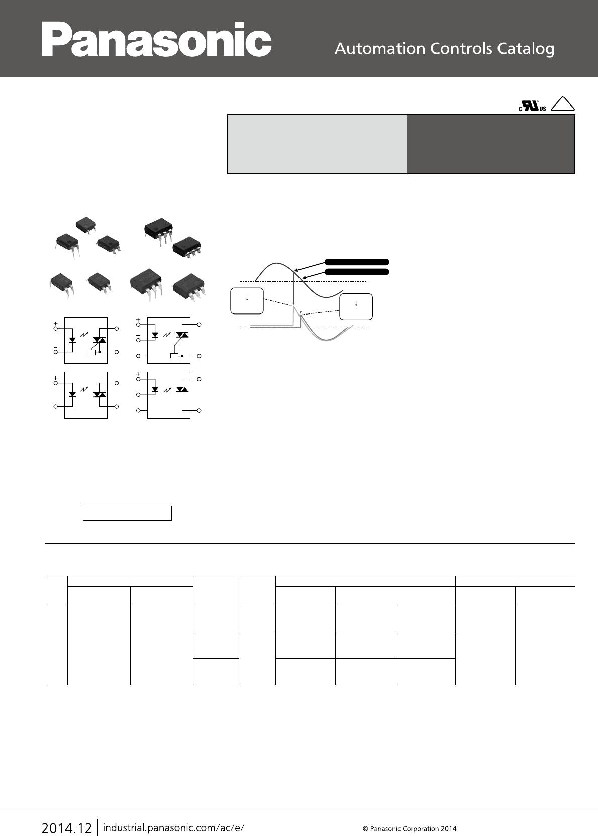
1) Zero-cross type (max. 50V) and random type
Notes: 1. For type of connection, see page 9.
2. Terminals are either solder plated or solder dipped.
Item Symbol APT1211(W), APT1221(W), APT1231(W), APT1212(W), APT1222(W), APT1232(W) Remarks
Input
LED forward current I
F 50 mA
LED reverse voltage VR 6 V
Peak forward current I
FP 1 A
f = 100 Hz,
Duty Ratio = 0.1%
Output
Repetitive peak
OFF-state voltage
V
DRM 600 V
ON-state RMS current* I
T(RMS) 0.1 A AC
Non-repetitive surge
current
I
TSM 1.2 A In one cycle at 60Hz
Total power dissipation P
T 500 mW
I/O isolation voltage Viso 5,000 V AC
Temperature limits
Operating T
opr –40°C to +100°C –40°F to +212°F
Non-condensing at
low temperatures
Storage T
stg –40°C to +125°C –40°F to +257°F
Item Symbol APT1211S, APT1211(W), APT1212(W) APT1221S, APT1221(W), APT1222(W) Condition
Input
LED dropout voltage
Typical
V
F
1.21 V
IF = 20 mA
Maximum 1.3 V
LED reverse current
Typical
IR
—
VR = 6 V
Maximum 10 μA
Output
Repetitive peak
OFF-state current
Typical
IDRM
—
I
F = 0 mA
V
DRM = 600 V
Maximum 1 μA
Repetitive peak
On-state voltage
Typical
V
TM
1.3 V
I
F = 10 mA
I
TM = 0.05 A
Maximum 2.5 V
Holding current
Typical
I
H
0.3 mA
Maximum 3.5 mA
Critical rate of rise of
OFF-state voltage
Minimum dv/dt 500 V/μsV
DRM = 600 V ×1/M2
Transfer
characteristics
Trigger LED current Maximum I
FT 10 mA
V
D = 6 V
R
L = 100 Ω
Zero-cross voltage Maximum VZC 50 V — IF = 10 mA
Turn on time* Maximum T
on 100 μs
I
F = 20 mA
V
D = 6 V
R
L = 100 Ω
I/O capacitance Maximum C
iso 1.5 pF
f = 1 MHz
V
B = 0 V
I/O isolation resistance Minimum Riso 50 GΩ 500 V DC
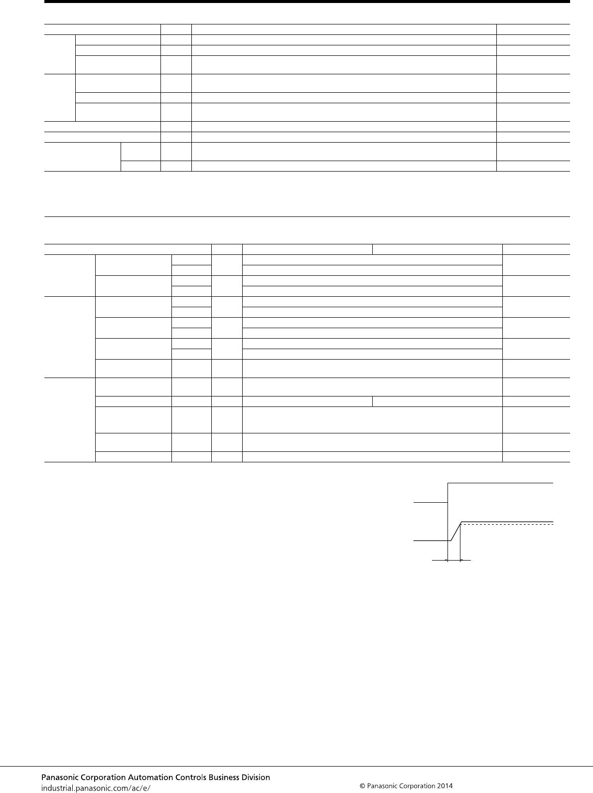
*Turn on time
Input
Output
To n
90%