BU9253FS-E2

4
Multimedia ICs BU9253AS / BU9253FS / BU9255FS
Measurement circuit (for BU9253FS / BU9255FS)
VCC
VCC
100µ
0.1µ
0.01µ
0.012µ
2.2µ
20k
8.2k
1k
2.2µ
IN1
IN2
1k
4700p
10k
100p
39k
MIX
2.2µ
22k
RESISTOR : []
Unit
CAPACITOR: [F]
OUT
3300p
15k10k
4.7k
0.01µ
0.01µ
22µ
V
CC
1
2
34
5678
0.47µ
D / A
SRAM
A / DOSC
16 15
14
13
12 11
10
9
COUNTER
+
+
Fig. 1
5
Multimedia ICs BU9253AS / BU9253FS / BU9255FS
• When switching between the muted and unmuted
state (pin 15 (pin 17) LMH), the pin 15 (pin 17) M
time should be longer than one SRAM cycle. This is to
assure stability by initializing the SRAM before mode
switching.
Note: Figures in parentheses ( ) are for BU9253AS.
(2) Differences between BU9253AS / FS and BU9255FS
There is a difference regarding the signal stopping for
muting. With BU9253AS / FS, the output from pin 8 (pin
9) is stopped during muting. With BU9255FS, the output
from pin 5 is stopped during muting.
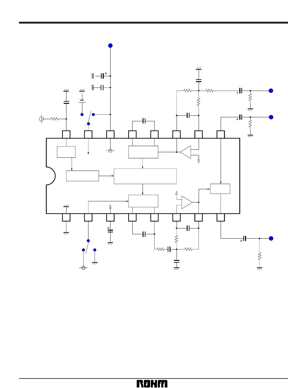
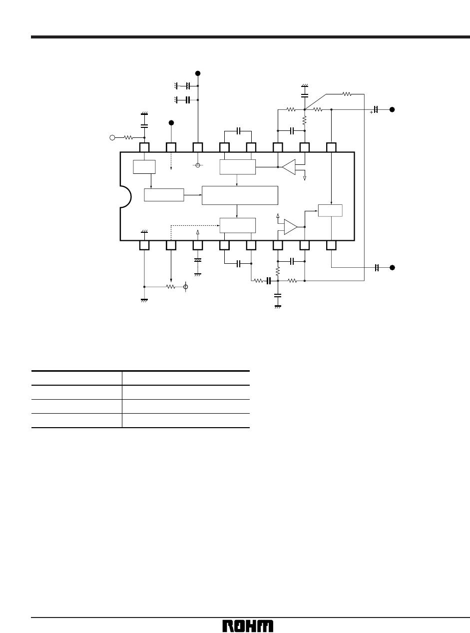
Application example (for BU9253FS / BU9255FS)
VCC
VCC
100µ
0.1µ
0.01µ
0.012µ
20k
20k
8.2k
IN
4700p
10k
100p
39k
MUTE
MIX
2.2µ
2.2µ
RESISTOR : []
Unit
CAPACITOR: [F]
OUT
3300p
15k
10k
4.7k
0.01µ
0.01µ
22µ
ECHO LEVEL
12345678
0.47µ
D / A
SRAM
A / D
OSC
16 15 14 13 12 11 10 9
COUNTER
Fig. 2
+
+
+
+
+
(1) Mute control functions
H Unmuted (operating state)
M Muted
L Clock stop and muted
Pin 15 voltage (pin 17) Mode
6
Multimedia ICs BU9253AS / BU9253FS / BU9255FS
External dimensions (Units: mm)
SSOP-A16
0.51Min.
0° ~ 15°
7.62
3.95 ± 0.3
1.778
10
9
6.5 ± 0.3
19.4 ± 0.3
18
1
0.5 ± 0.1
3.4 ± 0.2
0.3
± 0.1
SDIP18
BU9253ASBU9253FS / BU9255FS
0.36 ± 0.10.8
0.11
6.6 ± 0.2
4.4 ± 0.2
6.2 ± 0.31.5 ± 0.1
1
16
8
9
0.15
0.3Min.
0.15 ± 0.1
(3) Setting the echo loop gain
VIN
LPF
R
R
AD SRAM
OdB
V
IN
VO
VDLY
Recommendable gain
+ 3dB
Recommendable gain
– 6dB
R: R = 1: 1
mix
Echo loop ATT V
IN ~ VDLY···A = (A < 1)
With Pin NO. BU9253FS
VIN
VDLY
OUT
DA
2
VR
9
7
8
Fig. 3
+
+
With VOMax being the maximum amplitude of VO at this
time (when the phases, including that of the DLY cir-
cuit, are in alignment):
Thus, maximum allowable input is the value of V
OMax
provided the specifications (1 = A). Assuming a feed-
back ratio (A) of 0.7 and a maximum V
OUT of 4.0 VP-P,
V
IN must be less than 1.2 VP-P.
V
OMax. = (1 + A + A2 + ···) VIN =
1
1-A
Σ
K = 0
A
K
· VIN = VIN

BU9253FS-E2

Mfr. #:
Manufacturer:
Description:
Video ICs ECHO CONTROL
Lifecycle:
New from this manufacturer.
Delivery:
DHL FedEx Ups TNT EMS
Payment:
T/T Paypal Visa MoneyGram Western Union

Products related to this Datasheet