Data Sheet AD8613/AD8617/AD8619
Rev. H | Page 5 of 16
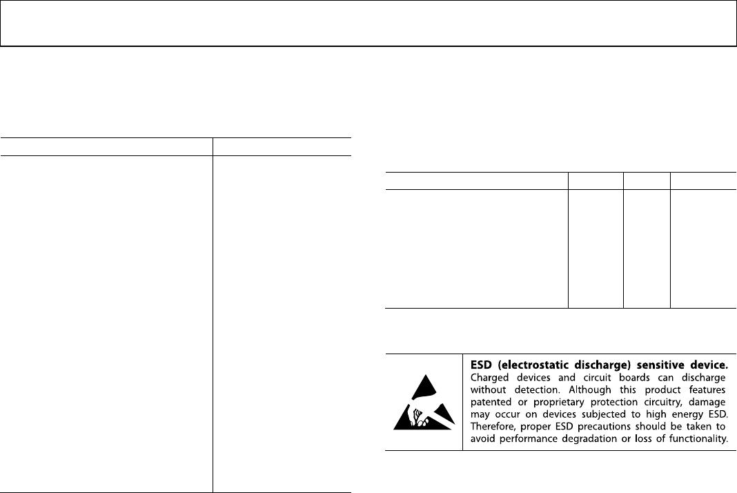
ABSOLUTE MAXIMUM RATINGS
T
A
= 25°C, unless otherwise noted.
Table 3.
Parameter Rating
Supply Voltage 6 V
Input Voltage V
SS
− 0.3 V to V
DD
+ 0.3 V
Input Current ±10 mA
Differential Input Voltage ±6 V
Output Short-Circuit Duration to GND Indefinite
Storage Temperature Range −65°C to +150°C
Operating Temperature Range −40°C to +125°C
Junction Temperature Range −65°C to +150°C
Lead Temperature (Soldering, 60 sec) 300°C
ESD AD8613
HBM ±4000 V
FICDM ±1000 V
ESD AD8617
HBM ±3000 V
FICDM ±1000 V
MM ±100 V
ESD AD8619
HBM ±4000 V
FICDM ±1250 V
MM ±200 V
Stresses at or above those listed under Absolute Maximum
Ratings may cause permanent damage to the product. This is a
stress rating only; functional operation of the product at these
or any other conditions above those indicated in the operational
section of this specification is not implied. Operation beyond
the maximum operating conditions for extended periods may
affect product reliability.
THERMAL RESISTANCE
θ
JA
is specified for the worst-case conditions, that is, a device
soldered in a circuit board for surface-mount packages.
Table 4. Thermal Characteristics
Package Type θ
JA
θ
JC
Unit
5-Lead TSOT-23 (UJ-5) 207 61 °C/W
5-Lead SC70 (KS-5) 376 126 °C/W
8-Lead MSOP (RM-8) 210 45 °C/W
8-Lead SOIC_N (R-8) 158 43 °C/W
8-Lead LFCSP (CP-8-21) 81 20 °C/W
14-Lead SOIC_N (R-14) 120 36 °C/W
14-Lead TSSOP (RU-14) 180 35 °C/W
ESD CAUTION