ZL40215 Data Sheet
16
Microsemi Corporation
* The VOD parameter was measured from 125 MHz to 750 MHz.
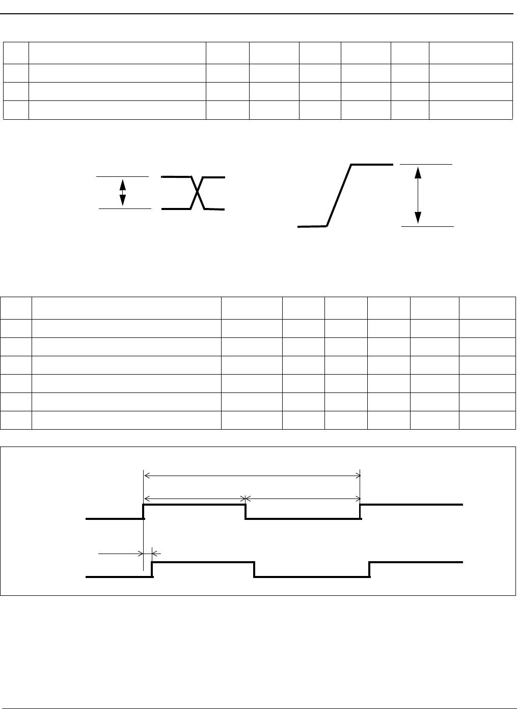
Figure 19 - Differential Voltage Parameter
* Supply voltage and operating temperature are as per Recommended Operating Conditions
Input
t
P
t
REFW
t
pd
t
REFW
Output
Figure 20 - Input To Output Timing
7 Differential input resistance V
IR
80 100 120 ohm
8 LVDS output differential voltage* V
OD
0.25 0.30 0.40 V
9 LVDS output common mode voltage V
CM
1.1 1.25 1.375 V
2*V
OD
V
OD
AC Electrical Characteristics* - Inputs and Outputs (see Figure 20) - for 2.5/3.3 V supply.
Characteristics Sym. Min. Typ. Max. Units Notes
1 Maximum Operating Frequency 1/t
p
750 MHz
2 input to output clock propagation delay t
pd
0 1 2 ns
3 output to output skew t
out2out
50 100 ps
4 part to part output skew t
part2part
80 300 ps
5 Output clock Duty Cycle degradation t
PWH
/ t
PWL
-5 0 5 %
6 LVDS Output slew rate r
sl
0.55 V/ns
DC Electrical Characteristics - Inputs and outputs - for 2.5/3.3 V supply
Cha
racteristics Sym. Min. Typ. Max. Units Notes
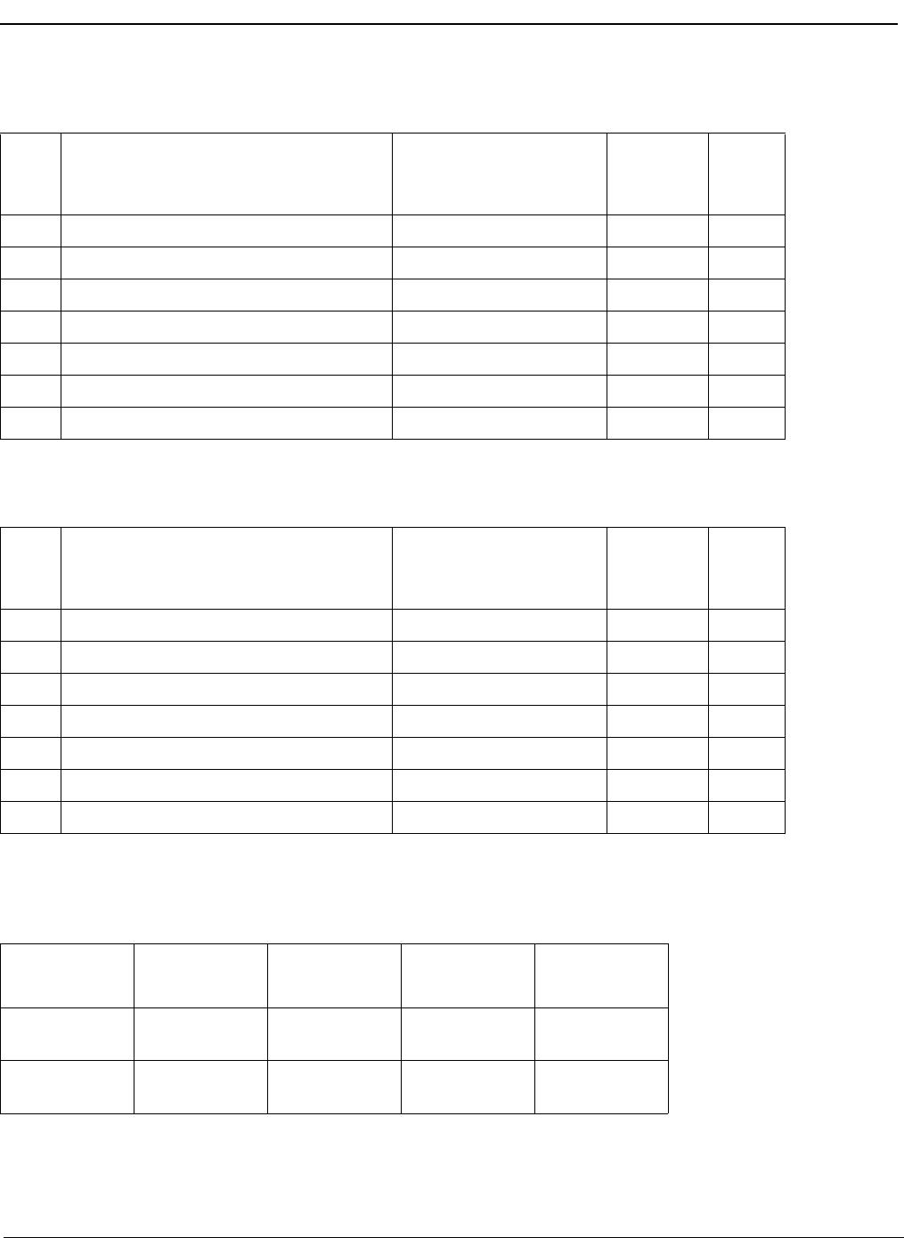
Additive Jitter at 3.3 V*
Output Frequency (MHz)
Jitter
Measurement
Filter
Typical
(f
s)
Notes
1 125 12 kHz - 20 MHz 123
2 212.5 12 kHz - 20 MHz 104
3 311.04 12 kHz - 20 MHz 92
4 425 12 kHz - 20 MHz 94
5 500 12 kHz - 20 MHz 78
6 622.08 12 kHz - 20 MHz 79
7 750 12 kHz - 20 MHz 80
ZL40215 Data Sheet
17
Microsemi Corporation
5.0 Performance Characterization
* For an input slew rate of approximately 0.8 V/ns.
Additive jitter in the presence of power supply noise*
Carrier
f
requency
Parameter Typical Units Notes
125 25 mV
at 100 kHz
38 fs RMS
750 25 mV
at 100 kHz
50 fs RMS
* The values in this table are the additive periodic jitter caused by an interfering tone typically caused by a switching power supply. For this test,
measurements were taken over the full temperature and voltage range for V
DD
= 3.3 V. The magnitude of the interfering tone is measured at the
DUT.
Additive Jitter at 2.5 V*
Output Frequency (MHz)
Jitter
Measurement
Filter
Typical
(fs)
Notes
1 125 12 kHz - 20 MHz 120
2 212.5 12 kHz - 20 MHz 102
3 311.04 12 kHz - 20 MHz 88
4 425 12 kHz - 20 MHz 91
5 500 12 kHz - 20 MHz 77
6 622.08 12 kHz - 20 MHz 78
7 750 12 kHz - 20 MHz 78
ZL40215 Data Sheet
18
Microsemi Corporation
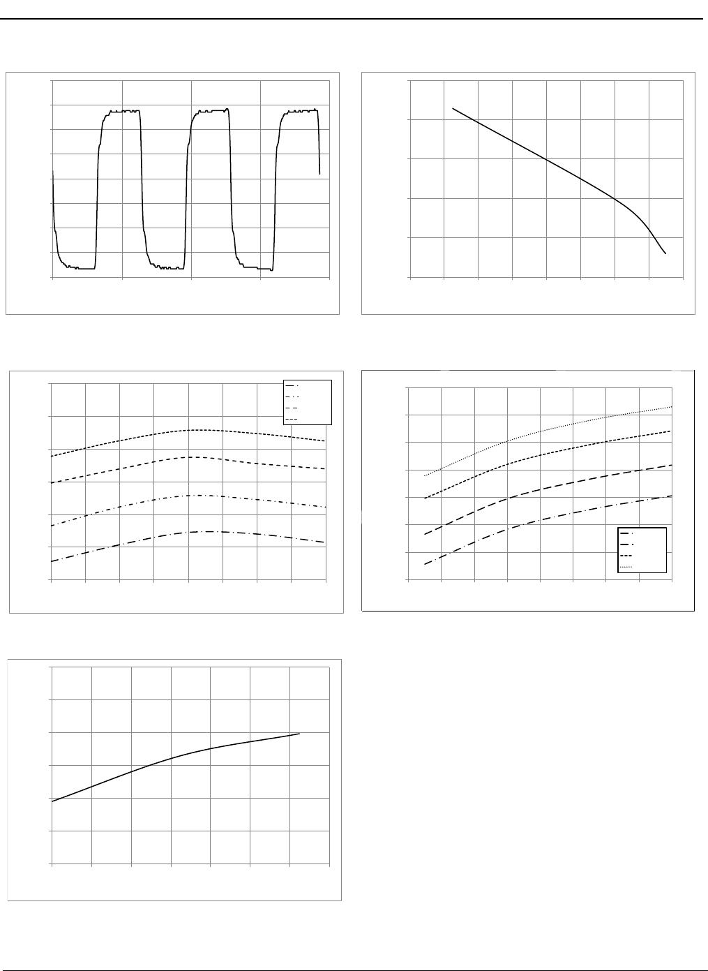
6.0 Typical Behavior
Typical Waveform at 155.52 MHz V
OD
versus Frequency
Power Supply Tone Frequency versus PSRR Power Supply Tone Magnitude versus PSRR
Propagation Delay versus Temperature
Note: This is for a single device. For more details see the
characterization section.
-0.2
-0.15
-0.1
-0.05
0
0.05
0.1
0.15
0.2
0 5 10 15 20
Voltage
Time (ns)
0.305
0.31
0.315
0.32
0.325
0.33
0 100 200 300 400 500 600 700 800
Voltage
Frequency (MHz)
-90
-85
-80
-75
-70
-65
-60
100 150 200 250 300 350 400 450 500
PSRR (dBc)
Power Supply Tone Frequency with 25 mV (kHz)
125 MHz
212.5 MHz
425 MHz
750 MHz
-90
-85
-80
-75
-70
-65
-60
-55
20 30 40 50 60 70 80 90 100
PSRR (dBc)
Power Supply Tone magnitude (mV) at 100 kHz
125 MHz
212.5 MHz
425 MHz
750 MHz
0.3
0.35
0.4
0.45
0.5
0.55
0.6
-40 -20 0 20 40 60 80 100
Propagation Delay (ns)
Temperature (°C)

ZL40215LDF1

Mfr. #:
Manufacturer:
Microchip / Microsemi
Description:
Clock Buffer 1:4 LVDS Fanout Buffer w/Int. Term.
Lifecycle:
New from this manufacturer.
Delivery:
DHL FedEx Ups TNT EMS
Payment:
T/T Paypal Visa MoneyGram Western Union

Products related to this Datasheet