IRF6726MTRPBF

www.irf.com 1
08/14/07
IRF6726MPbF
IRF6726MTRPbF
DirectFET Power MOSFET
Description
The IRF6726MPbF combines the latest HEXFET® Power MOSFET Silicon technology with the advanced DirectFET
TM
packaging to achieve
the lowest on-state resistance in a package that has the footprint of a MICRO-8 and only 0.7 mm profile. The DirectFET package is
compatible with existing layout geometries used in power applications, PCB assembly equipment and vapor phase, infra-red or convection
soldering techniques, when application note AN-1035 is followed regarding the manufacturing methods and processes. The DirectFET pack-
age allows dual sided cooling to maximize thermal transfer in power systems, improving previous best thermal resistance by 80%.
The IRF6726MPbF balances both low resistance and low charge along with ultra low package inductance to reduce both conduction and
switching losses. The reduced total losses make this product ideal for high efficiency DC-DC converters that power the latest generation of
processors operating at higher frequencies. The IRF6726MPbF has been optimized for parameters that are critical in synchronous buck
operating from 12 volt bus converters including Rds(on) and gate charge to minimize losses.
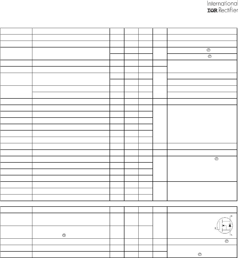
Applicable DirectFET Outline and Substrate Outline (see p.7,8 for details)
Fig 1. Typical On-Resistance vs. Gate Voltage
Typical values (unless otherwise specified)
Fig 2. Typical Total Gate Charge vs. Gate-to-Source Voltage
Click on this section to link to the appropriate technical paper.
Click on this section to link to the DirectFET Website.
Surface mounted on 1 in. square Cu board, steady state.
T
C
measured with thermocouple mounted to top (Drain) of part.
Repetitive rating; pulse width limited by max. junction temperature.
Starting T
J
= 25°C, L = 0.82mH, R
G
= 25, I
AS
= 25A.
Notes:
DirectFET ISOMETRIC
MT
PD - 96121
l RoHS Compliant Containing No Lead and Bromide
l Low Profile (<0.7 mm)
l Dual Sided Cooling Compatible
l Ultra Low Package Inductance
l Optimized for High Frequency Switching
l Ideal for CPU Core DC-DC Converters
l Optimized for both Sync.FET and some Control FET
application
l Low Conduction and Switching Losses
l Compatible with existing Surface Mount Techniques
l 100% Rg tested
SQ SX ST MQ MX
MT
MP
0 5 10 15 20
V
GS,
Gate -to -Source Voltage (V)
0
1
2
3
4
T
y
p
i
c
a
l
R
D
S
(
o
n
)
(
m
)
I
D
= 32A
T
J
= 25°C
T
J
= 125°C
0 102030405060
Q
G
,
Total Gate Charge (nC)
0.0
1.0
2.0
3.0
4.0
5.0
V
G
S
,
G
a
t
e
-
t
o
-
S
o
u
r
c
e
V
o
l
t
a
g
e
(
V
)
V
DS
= 24V
V
DS
= 15V
I
D
= 25A
Absolute Maximum Ratin
g
s
Parameter Units
V
DS
Drain-to-Source Voltage V
V
GS
Gate-to-Source Voltage
I
D
@ T
A
= 25°C
Continuous Drain Current, V
GS
@ 10V
I
D
@ T
A
= 70°C
Continuous Drain Current, V
GS
@ 10V
A
I
D
@ T
C
= 25°C
Continuous Drain Current, V
GS
@ 10V
I
DM
Pulsed Drain Current
E
AS
Single Pulse Avalanche Energy mJ
I
AR
Avalanche Current A
Max.
25
180
250
±20
30
32
260
25
V
DSS
V
GS
R
DS(on)
R
DS(on)
30V max ±20V max
1.3m@10V 1.9m@ 4.5V
Q
g tot
Q
gd
Q
gs2
Q
rr
Q
oss
V
gs(th)
51nC 16nC 5.4nC 45nC 28nC 1.7V
IRF6726MPbF
2 www.irf.com
Pulse width 400µs; duty cycle 2%.
Notes:
Static @ T
J
= 25°C (unless otherwise specified)
Parameter Min. Typ. Max. Units
BV
DSS
Drain-to-Source Breakdown Voltage 30 ––– ––– V
∆ΒV
DSS
/T
J
Breakdown Voltage Temp. Coefficient ––– 21 ––– mV/°C
R
DS(on)
Static Drain-to-Source On-Resistance ––– 1.3 1.7
m
––– 1.9 2.4
V
GS(th)
Gate Threshold Voltage 1.35 1.7 2.35 V
V
GS(th)
/T
J
Gate Threshold Voltage Coefficient ––– -6.0 ––– mV/°C
I
DSS
Drain-to-Source Leakage Current ––– ––– 1.0 µA
––– ––– 150
I
GSS
Gate-to-Source Forward Leakage ––– ––– 100 nA
Gate-to-Source Reverse Leakage ––– ––– -100
gfs Forward Transconductance 150 ––– ––– S
Q
g
Total Gate Charge ––– 51 77
Q
gs1
Pre-Vth Gate-to-Source Charge ––– 12 –––
Q
gs2
Post-Vth Gate-to-Source Charge ––– 5.4 ––– nC
Q
gd
Gate-to-Drain Charge ––– 16 –––
Q
godr
Gate Charge Overdrive ––– 18 ––– See Fig. 15
Q
sw
Switch Charge (Q
gs2
+ Q
gd
)
––– 21 –––
Q
oss
Output Charge ––– 28 ––– nC
R
G
Gate Resistance ––– 1.0 1.8
t
d(on)
Turn-On Delay Time ––– 20 –––
t
r
Rise Time ––– 30 ––– ns
t
d(off)
Turn-Off Delay Time ––– 25 –––
t
f
Fall Time ––– 17 –––
C
iss
Input Capacitance ––– 6140 –––
C
oss
Output Capacitance ––– 1270 ––– pF
C
rss
Reverse Transfer Capacitance ––– 590 –––
Diode Characteristics
Parameter Min. Typ. Max. Units
I
S
Continuous Source Current ––– ––– 110
(Body Diode) A
I
SM
Pulsed Source Current ––– ––– 250
(Body Diode)
V
SD
Diode Forward Voltage ––– 0.77 1.0 V
t
rr
Reverse Recovery Time ––– 27 41 ns
Q
rr
Reverse Recovery Charge ––– 45 68 nC
di/dt = 500A/µs
T
J
= 25°C, I
S
= 25A, V
GS
= 0V
showing the
integral reverse
p-n junction diode.
V
GS
= 4.5V, I
D
= 25A
V
DS
= V
GS
, I
D
= 150µA
T
J
= 25°C, I
F
= 25A
V
GS
= 4.5V
I
D
= 25A
V
GS
= 0V
V
DS
= 15V
I
D
= 25A
V
DD
= 15V, V
GS
= 4.5V
Conditions
V
GS
= 0V, I
D
= 250µA
Reference to 25°C, I
D
= 1mA
V
GS
= 10V, I
D
= 32A
V
GS
= 20V
V
GS
= -20V
V
DS
= 24V, V
GS
= 0V
V
DS
= 15V
V
DS
= 24V, V
GS
= 0V, T
J
= 125°C
MOSFET symbol
R
G
= 1.8
V
DS
= 15V, I
D
= 25A
Conditions
See Fig. 17
ƒ = 1.0MHz
V
DS
= 16V, V
GS
= 0V
IRF6726MPbF
www.irf.com 3
Fig 3. Maximum Effective Transient Thermal Impedance, Junction-to-Ambient
Used double sided cooling , mounting pad with large heatsink.
Mounted on minimum footprint full size board with metalized
back and with small clip heatsink.
Notes:
R
θ
is measured at T
J
of approximately 90°C.
Surface mounted on 1 in. square Cu
(still air).
Mounted to a PCB with
small clip heatsink (still air)
Mounted on minimum
footprint full size board with
metalized back and with small
clip heatsink (still air)
1E-006 1E-005 0.0001 0.001 0.01 0.1 1 10 100 1000
t
1
, Rectangular Pulse Duration (sec)
0.001
0.01
0.1
1
10
100
T
h
e
r
m
a
l
R
e
s
p
o
n
s
e
(
Z
t
h
J
A
)
0.20
0.10
D = 0.50
0.02
0.01
0.05
SINGLE PULSE
( THERMAL RESPONSE )
Notes:
1. Duty Factor D = t1/t2
2. Peak Tj = P dm x Zthja + Tc
Ri (°C/W) τi (sec)
1.1632 0.000194
5.4838 0.045124
21.2371 1.1955
17.1160 45.9
τ
J
τ
J
τ
1
τ
1
τ
2
τ
2
τ
3
τ
3
R
1
R
1
R
2
R
2
R
3
R
3
Ci= τi/Ri
Ci= τi/Ri
τ
A
τ
A
τ
4
τ
4
R
4
R
4
Absolute Maximum Ratin
g
s
Parameter Units
P
D
@T
A
= 25°C Power Dissipation W
P
D
@T
A
= 70°C
Power Dissipation
P
D
@T
C
= 25°C Power Dissipation
T
P
Peak Soldering Temperature °C
T
J
Operating Junction and
T
STG
Storage Temperature Range
Thermal Resistance
Parameter Typ. Max. Units
R
θJA
Junction-to-Ambient ––– 45
R
θJA
Junction-to-Ambient 12.5 –––
R
θJA
Junction-to-Ambient 20 ––– °C/W
R
θJC
Junction-to-Case ––– 1.4
R
θJ-PCB
Junction-to-PCB Mounted 1.0 ––
Linear Derating Factor
W/°C
0.022
270
-40 to + 150
Max.
89
2.8
1.8

IRF6726MTRPBF

Mfr. #:
Manufacturer:
Infineon / IR
Description:
MOSFET 30V 1 N-CH HEXFET DIRECTFET MX
Lifecycle:
New from this manufacturer.
Delivery:
DHL FedEx Ups TNT EMS
Payment:
T/T Paypal Visa MoneyGram Western Union

Products related to this Datasheet