ZL30107GGG2

1
Zarlink Semiconductor Inc.
Zarlink, ZL and the Zarlink Semiconductor logo are trademarks of Zarlink Semiconductor Inc.
Copyright 2007, Zarlink Semiconductor Inc. All Rights Reserved.
A full Data Sheet is available to qualified customers. To
register, please send an email to
TimingandSync@zarlink.com.
Features
Single chip low cost solution for synchronizing an
Ethernet PHY to a standard telecom clock
Generates an IEEE 802.3 jitter compliant 25 MHz
Gigabit Ethernet output clock
Supports three modes of operation:
Asynchronous Freerun, Synchronous, and
Asynchronous Holdover
Defaults in Asynchronous Freerun mode
In Asynchronous Freerun mode, the DPLL
generates an output clock with a frequency
accuracy equal to frequency accuracy of the
external crystal oscillator (XO) or a low cost
crystal (XTAL)
In Synchronous mode, the DPLL automatically
synchronizes to one of a pre-defined set of
frequencies including 2 kHz, 8 kHz, 64 kHz,
1.544 MHz, 2.048 MHz, 6.48 MHz, 8.192 MHz,
16.384 MHz, 19.44 MHz, 38.88 MHz, 77.76 MHz.
Configurable to accept a 25 MHz input reference
Automatic entry into Asynchronous Holdover
mode when all input references fail
Input reference is manually selectable through the
serial (SPI) interface
Hitless input reference switching
Lock indicator pin
Input reference status monitors
Programmable loop bandwidth of 14 Hz, 28 Hz, or
890 Hz
Applications
Ethernet Line Cards Supporting Synchronous
Transmission
March 2007
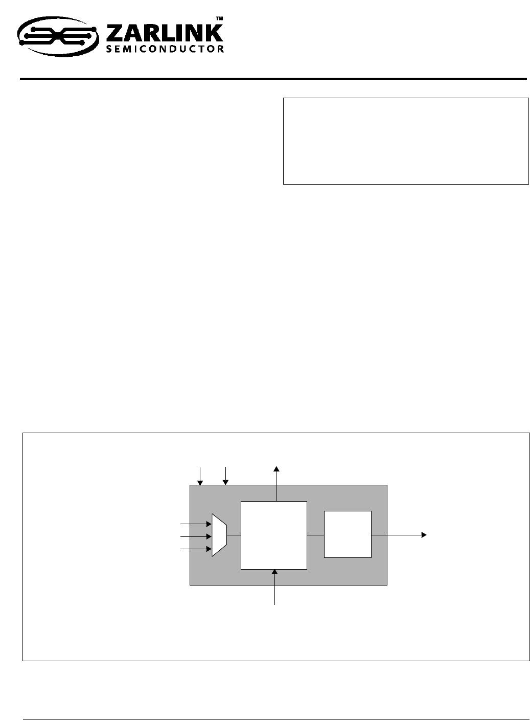
Figure 1 - Block Diagram
LOCK
CLK
X1/CLK
X2
uP I/F
DPLL
APLL
REF0
REF1
REF2
ZL30107
GbE Line Card Synchronizer
Shortform Data Sheet
Ordering Information
ZL30107GGG 64 Pin CABGA Trays
ZL30107GGG2 64 Pin CABGA* Trays
*Pb Free Tin/Silver/Copper
-40
o
C to +85
o
C
ZL30107 Shortform Data Sheet
2
Zarlink Semiconductor Inc.
Figure 2 - Pin Connections
B
C
D
E
F
G
H
12345678
1
1 - A1 corner is identified with a marking
A
V
SS
SISO
IC V
CORE
AV
CORE
IC IC IC V
DD
NC
IC
V
DD
AV
CORE
IC
CLKICV
SS
V
SS
V
SS
IC
IC
V
SS
X1/CLK
V
SS
V
SS
IC
V
SS
IC
RST
V
DD
IC IC REF1 IC LF1 AV
SS
IC AV
SS
REF0 IC IC REF2 LF2 AV
CORE
AV
DD
IC
SCK CS V
DD
AV
DD
LF3 AV
SS
V
DD
V
SS
V
CORE
V
DD
X2
IC V
SS
LOCK
V
DD
AV
SS
IC
9 mm x 9 mm
Ball Pitch 1.0 mm
ZL30107 Shortform Data Sheet
3
Zarlink Semiconductor Inc.
Pin Description
Pin # Name
I/O
Type
Description
B1
A3
B4
REF0
REF1
REF2
I
d
Reference Inputs (LVCMOS, Schmitt Trigger). These reference inputs are
used for synchronizing the PLL. These pins are internally pulled down to Vss.
D8 CLK O SONET/SDH/Ethernet Clock Output (LVCMOS). This output clock is
configurable as 77.76 MHz, 25 MHz, and 50 MHz. Default is 77.76 MHz.
G5 RST I Reset (LVCMOS, Schmitt Trigger). A logic low at this input resets the device. To
ensure proper operation, the device must be reset after power-up. Reset should
be asserted for a minimum of 300 ns.
E1 LOCK O Lock Indicator (LVCMOS). This is the lock indicator pin for the PLL. This output
goes high when the DPLL’s output is frequency is phase locked to the input
reference.
A5 LF1 A External Analog PLL Loop Filter terminal.
B5 LF2 A Analog PLL External Loop Filter Reference.
C5 LF3 A Analog PLL External Loop Filter Reference.
H4 X1/CLK I Oscillator Master Clock Input (LVCMOS). This input accepts a 20 MHz
reference from a clock oscillator (XO, XTAL). The stability and accuracy of the
clock at this input determines the free-run accuracy and the long term holdover
stability of the output clocks.
H5 X2 O Oscillator Master Clock Output (LVCMOS). This pin is used for connection
with an crystal. This pin must be left unconnected when the X1 pin is connected
to a clock oscillator.
C1 SCK I Clock for Serial Interface (LVCMOS). Serial interface clock.
D2 SI I Serial Interface Input (LVCMOS). Serial interface data input pin.
D1 SO O Serial Interface Output (LVCMOS). Serial interface data output pin.
C2 CS I
u
Chip Select for Serial Interface (LVCMOS). Serial interface chip select. This
pin is internally pulled up to Vdd.
F5
A1
A2
A4
A7
B8
D7
E2
G7
H1
B2
G4
G2
G3
G8
H3
F2
IC Internal Connection. Leave unconnected.

ZL30107GGG2

Mfr. #:
Manufacturer:
Microchip / Microsemi
Description:
Clock Generators & Support Products Pb Free GbE Line Card Synchronizer
Lifecycle:
New from this manufacturer.
Delivery:
DHL FedEx Ups TNT EMS
Payment:
T/T Paypal Visa MoneyGram Western Union

Products related to this Datasheet