Expand menu
Hello, Sign in
My Account
0
Cart
Home
Products
Sensors
Semiconductors
Passive Components
Connectors
Power
Electromechanical
Optoelectronics
Circuit Protection
Integrated Circuits - ICs
Main Products
Manufacturers
Blog
Services
About OMO
About Us
Contact Us
Check Stock
PL123-05NSC
P1-P3
P4-P6
P7-P8
P
L
1
2
3
-
0
5
N
/
-
09
N
L
o
w
S
k
e
w
F
a
n
o
u
t
B
u
f
f
e
r
M
ic
r
e
l
I
n
c
.
•
2
1
8
0
F
o
rt
u
n
e
D
r
i
v
e
•
S
a
n
J
o
s
e
,
C
A
9
5
1
3
1
•
U
S
A
•
t
e
l
+
1
(
4
0
8
)
9
4
4
-
0
8
0
0
•
f
a
x
+
1
(
4
0
8
)
4
7
4
-
1
0
0
0
•
w
w
w
.
m
i
c
r
e
l
.
c
o
m
R
e
v
0
3
/
1
5
/1
2
P
a
g
e
4
E
L
E
C
T
R
I
C
A
L
C
H
A
R
A
C
T
E
R
I
S
T
I
C
S
(
C
om
m
erc
i
al
an
d
I
nd
u
st
r
i
a
l
T
em
p
e
r
at
u
r
e
D
e
v
i
c
es
)
P
ar
a
m
e
t
er
De
s
c
r
i
p
t
io
n
T
e
st
C
o
n
d
i
ti
o
n
s
M
in
.
M
ax
.
Un
i
t
V
I
L
Input L
OW
Vol
t
age
[1]
V
DD
> 2.25V
–
0.8
V
V
IH
Input H
IGH Vo
l
t
age
[1]
V
DD
> 2.25V
2.
0
–
V
I
IL
Input L
OW Curr
ent
V
IN
= 0V
–
50
µA
I
IH
Input H
IGH Curr
ent
V
IN
= V
DD
–
100
µA
V
OL
Output LO
W Vo
l
t
age
[2]
I
OL
= 8 mA , V
DD
> 2.97V
–
0.4
V
V
OH
Output H
IG
H
Volt
age
[2]
I
OH
=
–
8 m
A
,
V
DD
> 2.97V
2.4
–
V
I
DD
Supply Cur
rent
66.67M
Hz with u
nl
oa
ded out
puts
–
32
mA
S
WI
T
C
H
IN
G
C
H
AR
A
CT
E
R
IS
T
IC
S
(
C
om
m
erc
i
al
a
nd
I
n
d
u
st
r
i
a
l
T
em
p
e
r
at
u
r
e
D
e
vi
c
es
)
[
3
]
Parameter
Desc
ription
Test C
on
d
it
ions
Min.
Typ
.
Max.
Unit
Duty C
ycle
[2]
= t2 ÷ t1
Measur
ed at 1.4V
,
V
DD
=3.3V, Inpu
t=50
%
40
50
60
%
Measur
ed at V
DD
/2
, Inpu
t = 50
%
40
50
60
%
t
3
Rise
T
ime
[2]
0.8V
2.0
V
,
V
DD
=3.3V , 30p
F Load
–
–
1.5
ns
10%
90
% , V
DD
=2.5V , 15pF
Load
–
–
2.5
ns
10%
90
% , V
DD
=1.8V , 15pF
Load
–
–
4.5
ns
t
4
Fall Time
[2]
2.0
V
0.8
V
,
V
DD
=3.3V , 30p
F Load
–
–
1
.5
ns
90%
10
% , V
DD
=2.5V , 15pF
Load
–
–
2.5
ns
90%
10
% , V
DD
=1.8V , 15pF
Load
–
–
4.5
ns
t
5
Output to O
utput S
kew
[2]
All
o
utpu
ts
eq
ua
lly loade
d
–
–
250
ps
t
6
Propa
gation Dela
y
,
RE
F Rising
Edge to C
LKX
Ri
s
i
ng Ed
ge
[2]
Measure
d at V
DD
/2
1
5
9.2
ns
N
o
t
e
s:
1
.
R
EF
in
p
u
t
h
a
s
a
th
r
e
sh
o
l
d
vo
l
t
a
ge
o
f
V
DD
/2
2
.
P
ar
am
e
t
er
i
s
gu
ar
an
t
e
e
d
b
y
d
e
s
i
g
n
a
n
d
ch
ar
a
c
t
e
r
i
z
a
t
io
n
.
N
ot
1
0
0
%
t
e
s
te
d
in
p
r
o
d
u
c
t
io
n
.
3
.
A
l
l
p
ar
am
e
te
r
s
ar
e
sp
e
c
i
f
i
e
d
w
i
th
l
o
ad
e
d
o
u
t
p
u
t
s
.
P
L
1
2
3
-
0
5
N
/
-
09
N
L
o
w
S
k
e
w
F
a
n
o
u
t
B
u
f
f
e
r
M
ic
r
e
l
I
n
c
.
•
2
1
8
0
F
o
rt
u
n
e
D
r
i
v
e
•
S
a
n
J
o
s
e
,
C
A
9
5
1
3
1
•
U
S
A
•
t
e
l
+
1
(
4
0
8
)
9
4
4
-
0
8
0
0
•
f
a
x
+
1
(
4
0
8
)
4
7
4
-
1
0
0
0
•
w
w
w
.
m
i
c
r
e
l
.
c
o
m
R
e
v
0
3
/
1
5
/1
2
P
a
g
e
5
N
OIS
E
C
H
A
R
AC
T
E
RI
S
T
IC
S
(
C
om
m
er
c
i
al
a
nd
I
nd
u
st
r
i
a
l
T
em
p
er
at
u
r
e
D
e
vi
c
e
s)
Parameter
Desc
ription
Test C
on
d
it
ions
Min.
Typ
.
Max.
Unit
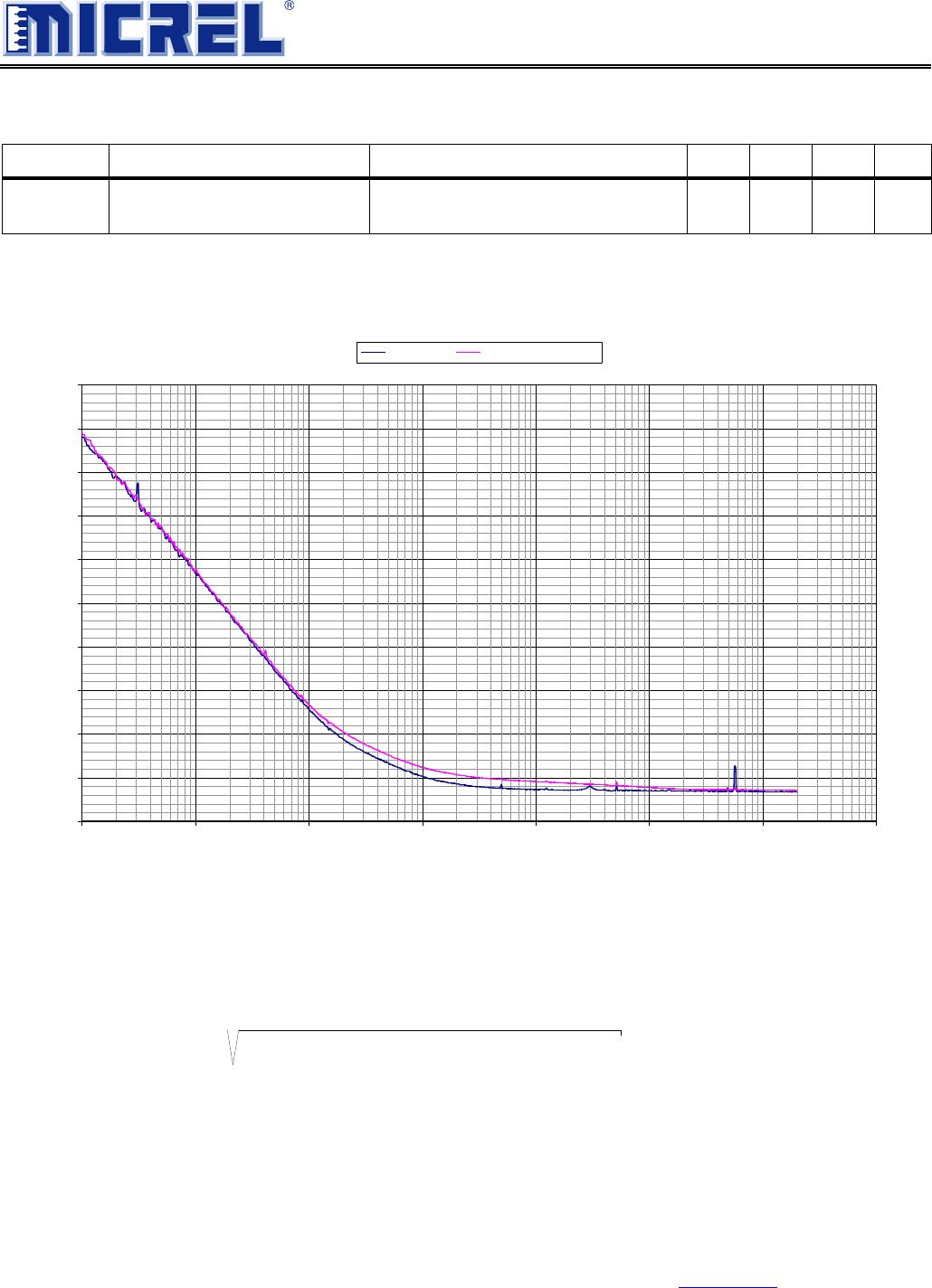
Additive Pha
s
e J
itter
V
DD
=3.3V, Freque
ncy=10
0MHz
Offset
=12KHz ~ 20
MHz
60
fs
PL123-09N Additiv
e P
hase Jitter:
VDD=3.3V, CLK=100MHz, Integration Range 12KHz to 20MHz: 0.0
59ps ty
pical.
-160
-150
-140
-130
-120
-110
-100
-90
-80
-70
-60
10
100
1000
10000
100000
1000000
10000000
100000000
Offset Frequency (Hz)
Phase Noise (dBc/Hz)
REF Input
PL123-09N Output
When a b
uffer i
s
u
s
ed
to
pas
s
a
s
i
gna
l the
n the buffe
r wi
ll
ad
d a
li
tt
l
e bit
of it
s own noi
se. Th
e phase noi
se on the o
utpu
t of the
buffer
wil
l be a
l
itt
le b
i
t m
ore t
han the pha
se noi
se i
n
the inpu
t sig
nal. To qu
ant
ify the n
oi
s
e a
d
dition
in the buffer
we c
ompare t
he
Phase J
i
tter
number
s
f
rom the
input and t
he output.
The dif
fere
nc
e
i
s ca
lled "Ad
ditive
Phase
Jitter".
The formu
l
a fo
r th
e
Add
it
i
ve
Phase J
i
tter
is as fo
llow
s
:
Ad
ditive
Phas
e Jit
ter
=
(O
utpu
t Pha
se Ji
tte
r) -
(Inpu
t Ph
ase
Jitte
r)
2
2
P
L
1
2
3
-
0
5
N
/
-
09
N
L
o
w
S
k
e
w
F
a
n
o
u
t
B
u
f
f
e
r
M
ic
r
e
l
I
n
c
.
•
2
1
8
0
F
o
rt
u
n
e
D
r
i
v
e
•
S
a
n
J
o
s
e
,
C
A
9
5
1
3
1
•
U
S
A
•
t
e
l
+
1
(
4
0
8
)
9
4
4
-
0
8
0
0
•
f
a
x
+
1
(
4
0
8
)
4
7
4
-
1
0
0
0
•
w
w
w
.
m
i
c
r
e
l
.
c
o
m
R
e
v
0
3
/
1
5
/1
2
P
a
g
e
6
S
W
I
T
C
H
I
N
G
W
A
VE
F
O
R
M
S
T
E
S
T
C
I
R
C
U
IT
1
.4
V
1
.4
V
t
2
t
1
VD
D
/2
IN
P
U
T
t
6
O
U
T
PU
T
VD
D
/2
1
.4
V
O
U
T
PU
T
t
5
O
U
T
PU
T
1
.4
V
D
u
t
y
C
y
c
le
T
i
m
i
ng
A
ll
O
u
t
p
ut
s
R
is
e
/
Fa
l
l
T
i
me
O
u
tp
u
t
-
O
u
t
p
u
t
Sk
e
w
In
p
u
t
-
O
ut
p
u
t
Pr
o
p
ag
a
t
i
on
D
e
l
a
y
t
3
t
4
O
U
T
PU
T
0
.8
V
2
.0
V
0V
3
.3
V
V
0
.8
V
2
.0
V
VD
D
VD
D
G
N
D
G
N
D
O
U
T
PU
T
S
C
L
O
A
D
CL
K
0
.1
F
0
.1
F
P1-P3
P4-P6
P7-P8
PL123-05NSC
Mfr. #:
Buy PL123-05NSC
Manufacturer:
Microchip Technology / Micrel
Description:
Clock Buffer DC - 134MHz 1:5 Fanout Buffer
Lifecycle:
New from this manufacturer.
Delivery:
DHL
FedEx
Ups
TNT
EMS
Payment:
T/T
Paypal
Visa
MoneyGram
Western
Union
Products related to this Datasheet
PL123-09NSC-R
PL123-05NSI
PL123-05NSC
PL123-09NSC
PL123-09NSI
PL123-05NSC-R
PL123-09NSI-R
PL123-05NSI-R
PL123-09NOC-R
PL123-09NOC