8
LTC1420
1420fa
Conversion Details
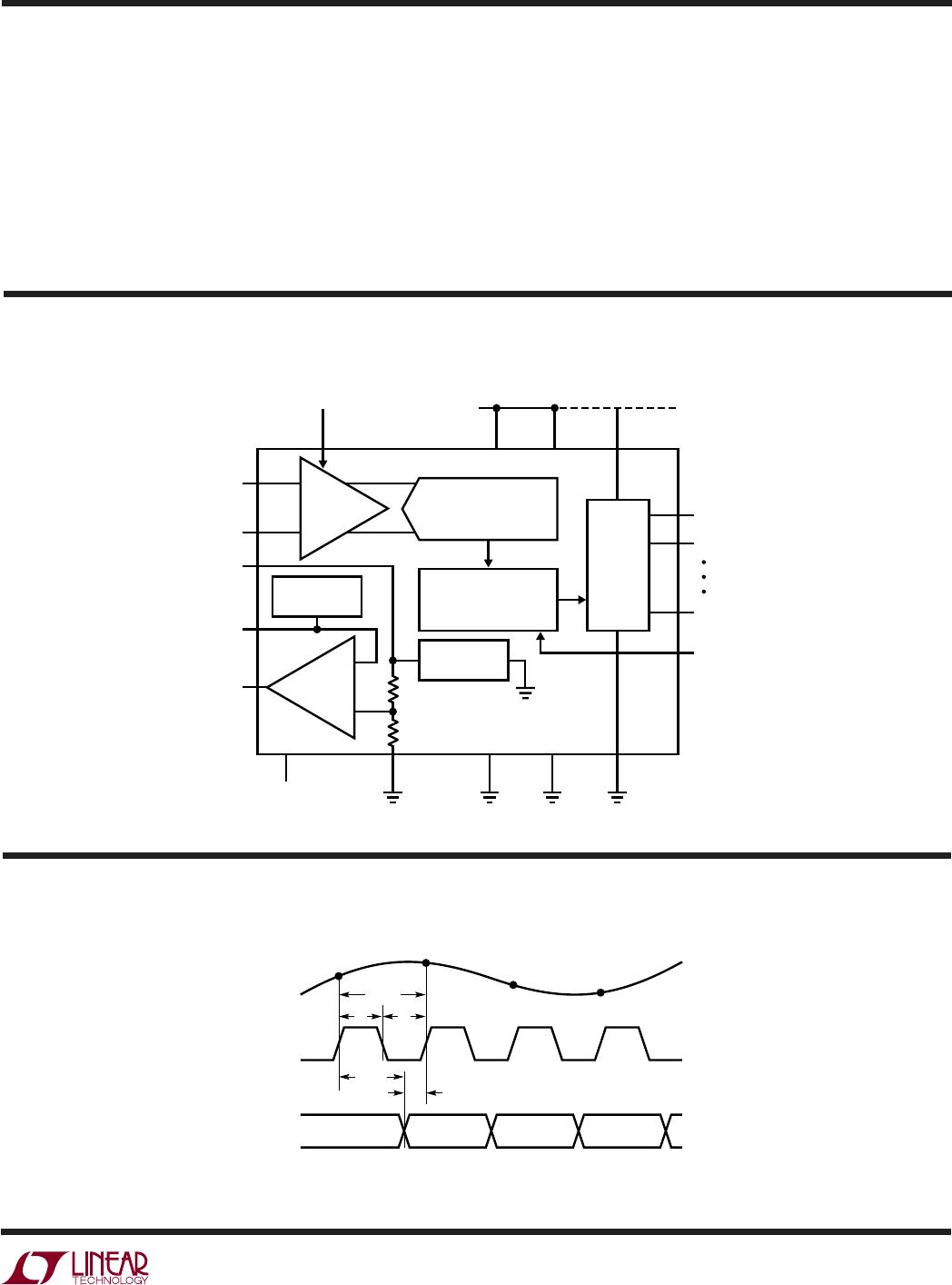
The LTC1420 is a high performance 12-bit A/D converter
that operates up to 10Msps. It is a complete solution with
an on-chip sample-and-hold, a 12-bit pipelined CMOS
ADC, a low drift programmable reference and an input
programmable gain amplifier. The digital output is paral-
lel, with a 12-bit two’s complement output and an out-of-
range (overflow) bit.
The rising edge of the CLK begins a conversion. The
differential analog inputs are simultaneously sampled and
passed on to the pipelined A/D. After two more conversion
starts (plus a 70ns conversion time) the digital outputs are
updated with the conversion result and will be ready for
capture on the third rising clock edge. Thus, even though
a new conversion is begun every time CLK goes high, each
result takes three clock cycles to reach the output.
The analog signals that are passed from stage to stage in
the pipelined A/D are stored on capacitors. The signals on
these capacitors will be lost if the delay between conver-
sions is too long. For accurate conversion results, the part
should be clocked faster than 20kHz.
In some pipelined A/D converters if there is no clock
present, dynamic logic on the chip will droop and the
power consumption sharply increases. The LTC1420
doesn’t have this problem. If the part is not clocked for
500µs, an internal timer will refresh the dynamic logic.
Thus, the clock can be turned off for long periods of time
to save power.
Power Supplies
The LTC1420 will operate from either a single 5V or dual
±5V supply, making it easy to interface the analog input to
single or dual supply systems. The digital output drivers
have their own power supply pin (OV
DD
) which can be set
from 3V to 5V, allowing direct connection to either 3V or
5V digital systems. For single supply operation, V
SS
should
be connected to analog ground. For dual supply operation,
V
SS
should be connected to –5V. Both V
DD
pins should be
connected to a clean 5V analog supply. (Don’t connect V
DD
to a noisy system digital supply.)
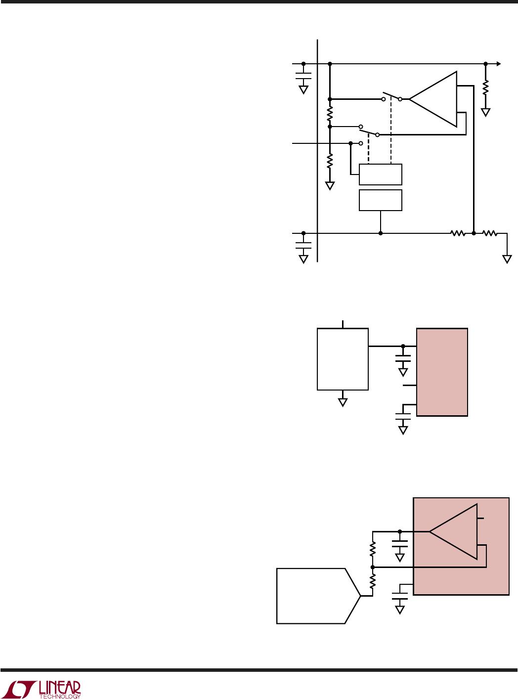
Analog Input Ranges
The LTC1420 has a flexible analog input with a wide
selection of input ranges. The input range is always
differential and is set by the voltages at the V
REF
and the
GAIN pins (Figure 1). The input range of the A/D core is
fixed at ±V
REF
/2. The reference voltage, V
REF
, is either set
by the on-chip voltage reference or directly driven by an
external voltage. The GAIN pin is a digital input that
controls the gain of a preamplifier in the sample-and-hold
circuit. The gain of this PGA can be set to 1× or 2×. Table 1
gives the input range in terms of V
REF
and GAIN.
Table 1
INPUT RANGE
GAIN PIN PGA GAIN (V
IN
= A
IN
+
– A
IN
–
)
5V (Logic H) 1× –V
REF
/2 < V
IN
< V
REF
/2
OV (Logic L) 2× –V
REF
/4 < V
IN
< V
REF
/4
V
REF
–A
IN
+A
IN
GAIN
1420 F01
1x/2x
V
IN
+
–
±V
REF
/2PGA S/H
ADC
CORE
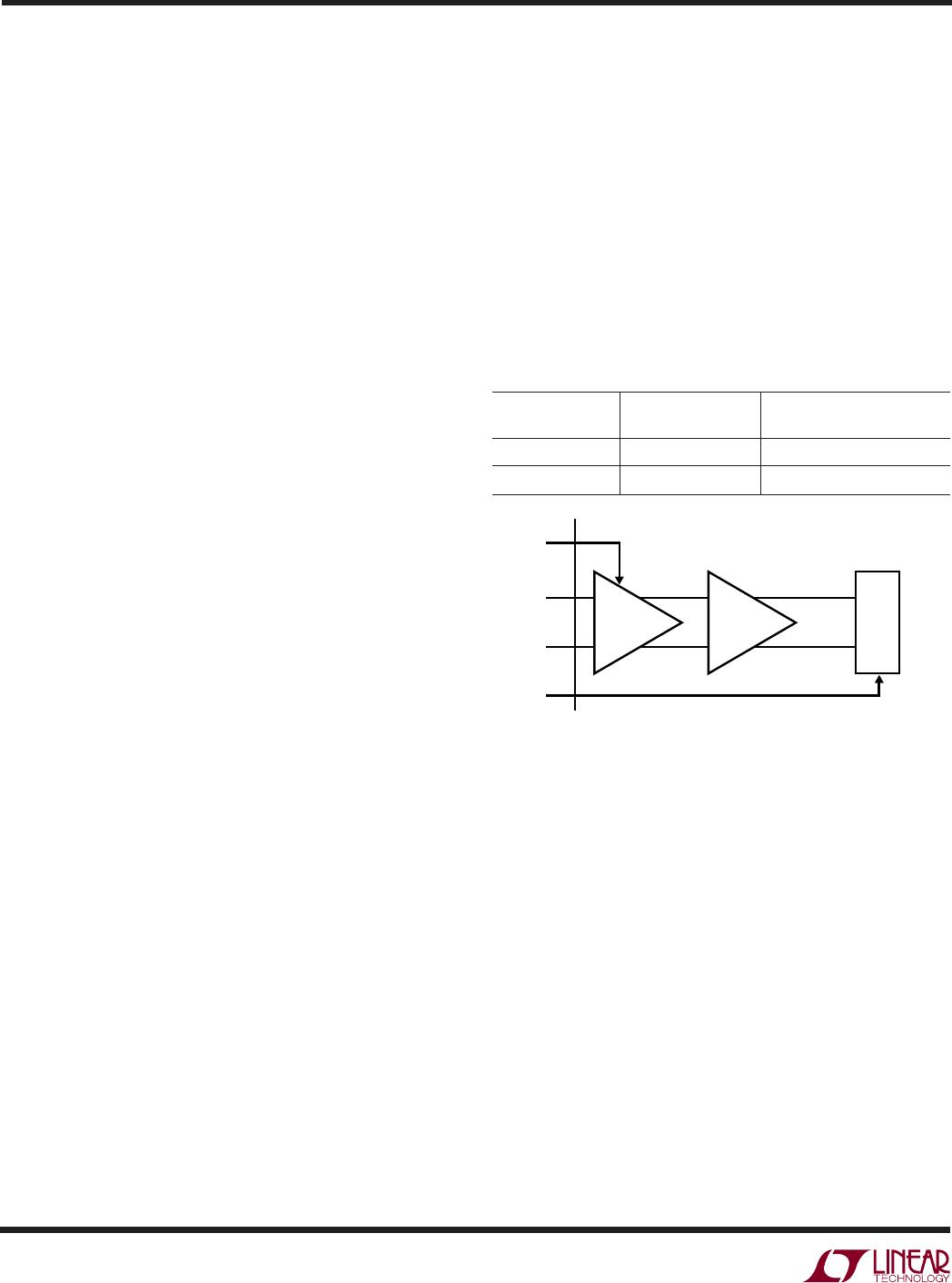
Internal Reference
Figure 2 shows a simplified schematic of the LTC1420
reference circuitry. An on-chip temperature compensated
bandgap reference (V
CM
) is factory trimmed to 2.500V.
The voltage at the V
REF
pin sets the input span of the ADC
to ±V
REF
/2. An internal voltage divider converts V
CM
to
2.048V, which is connected to a reference amplifier. The
reference programming pin, SENSE, controls how the
reference amplifier drives the V
REF
pin. If SENSE is tied to
ground, the reference amplifier feedback is connected to
the R1/R2 voltage divider, thus making V
REF
= 4.096V. If
SENSE is tied to V
REF
, the reference amplifier feedback is
connected to SENSE thus making V
REF
= 2.048V. If SENSE
is tied to V
DD
, the reference amplifier is disconnected from
Figure 1. Analog Input Circuit
APPLICATIONS INFORMATION
WUU
U