9DB833
EIGHT OUTPUT DIFFERENTIAL BUFFER FOR PCIE GEN1,2,3
IDT®
EIGHT OUTPUT DIFFERENTIAL BUFFER FOR PCIE GEN1,2,3 7
9DB833 REV H 06/07/16
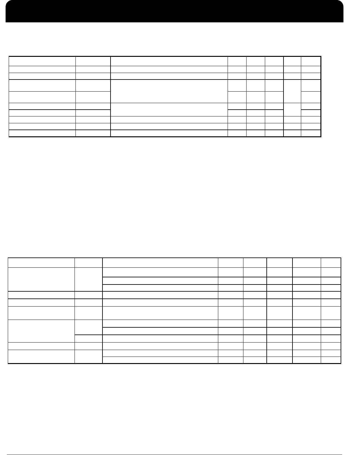
Electrical Characteristics–DIF 0.7V Current Mode Differential Outputs
Electrical Characteristics–Output Duty Cycle, Jitter, Skew and PLL Characteristics
T
A
= T
COM
or T
IND;
Supply Voltage VDD = 3.3 V +/-5%
PARAMETER SYMBOL CONDITIONS MIN TYP MAX UNITS NOTES
Slew rate Trf Scope avera
in
on 1.5 2.8 4
1, 2, 3
Slew rate matching
∆
Trf Slew rate matching, Scope averaging on 8 20
%
1, 2, 4
Voltage High VHigh 660 797 850 1
Voltage Low VLow -150 14 150 1
Max Volta
e Vmax 813 1150 1
Min Volta
eVmin -300-1 1
Vswing Vswing Scope averaging off (Differential) 300 1596.9 mV 1, 2
Crossin
Volta
e (abs) Vcross_abs Scope avera
in
off 250 378 550 mV 1, 5
Crossing Voltage (var)
∆
-Vcross Scope averaging off 16 140 mV 1, 6
2
Measured from differential waveform
6
The total variation of all Vcross measurements in any particular system. Note that this is a subset of V_cross_min/max (V_cross
absolute) allowed. The intent is to limit Vcross induced modulation by setting V_cross_delta to be smaller than V_cross absolute.
mV
Statistical measurement on single-ended signal
using oscilloscope math function. (Scope
averaging on)
Measurement on single ended signal using
absolute value. (Scope avera
in
off)
mV
1
Guaranteed by design and characterization, not 100% tested in production. IREF = VDD/(3xR
R
). For R
R
= 475
Ω
(1%), I
REF
= 2.32mA.
I
OH
= 6 x I
REF
and V
OH
= 0.7V @ Z
O
=50
Ω
(100
Ω
differential impedance).
3
Slew rate is measured through the Vswing voltage range centered around differential 0V. This results in a +/-150mV window around
differential 0V.
4
Matching applies to rising edge rate for Clock and falling edge rate for Clock#. It is measured using a +/-75mV window centered on
the average cross point where Clock rising meets Clock# falling. The median cross point is used to calculate the voltage thresholds the
oscilloscope is to use for the edge rate calculations.
5
Vcross is defined as voltage where Clock = Clock# measured on a component test board and only applies to the differential rising
edge (i.e. Clock rising and Clock# falling).
TA = T
COM
or T
IND;
Supply Voltage VDD = 3.3 V +/-5%
PARAMETER SYMBOL CONDITIONS MIN TYP MAX UNITS NOTES
-3dB point in High BW Mode (T
IND
) 1.5 2.8 4.1 MHz 1
-3dB point in High BW Mode (T
COM
-3dB point in Low BW Mode 0.7 1.1 1.4 MHz 1
JPEAK
Peak Pass band Gain 1.5 2 dB 1
Duty Cycle t
D
Measured differentially, PLL Mode 45 49.2 55 % 1
Duty Cycle Distortion t
DCD
Measured differentially, Bypass Mode @100MHz -2 -0.4 2 % 1,4
Bypass Mode, V
IND
) 3500 4263 4900 ps 1
Bypass Mode, V
COM
) 3500 4115 4500 ps 1,5
t
dPLL
= 50% -250 -45 250 ps 1
Skew, Output to Output t
sk3
PLL mode 21 50 ps 1,3
Additive Jitter in Bypass Mode 3 10 ps 1,3
1
Guaranteed by design and characterization, not 100% tested in production.
2
I
REF
= V
DD
/(3xR
R
). For R
R
= 475
Ω
(1%), I
REF
= 2.32mA. I
OH
= 6 x I
REF
and V
OH
= 0.7V @ Z
O
=50
Ω
.
3
Measured from differential waveform
4
Duty cycle distortion is the difference in duty cycle between the output and the input clock when the device is operated in bypass mode.
5
First number is commercial temp, second number is industrial temp.
Jitter, Cycle to cycle t
jcyc-cyc
PLL Bandwidth BW
Skew, Input to Output
t
pdBYP

