TBD62387A series
2017-03-21
Operating Ranges (Ta = −40 to 85°C, unless otherwise specified.)
Characteristics Symbol Test conditions Min Typ. Max Unit
Power supply voltage V
CC
― 4.5 5.0
5.5
V
Output voltage V
OUT
― ― ―
50
V
COMMON pin voltage V
COM
― 0 ―
V
Output
current
(per ch)
PG (Note1)
I
OUT
1 circuit ON, Ta = 25°C 0 ―
mA
t
pw
= 25 ms
8 circuits ON
Ta = 85°C
T
j
= 120°C
Duty = 10 % 0 ―
400
Duty = 50 % 0 ―
195
FNG (Note2)
1 circuit ON, Ta = 25°C 0 ―
400
t
pw
= 25 ms
8 circuits ON
Ta = 85°C
T
j
= 120°C
Duty = 10 % 0 ―
320
Duty = 50 % 0 ―
140
Input voltage (Output on) V
IN (ON)
I
OUT
= 100 mA or more, V
OUT
= 2 V 0 ―
V
CC
-3.5
V
Input voltage (Output off) V
IN (OFF)
I
OUT
= 100 μA or less, V
OUT
= 2 V V
CC
-0.4 ―
5.5
V
Clamp diode
forward current
I
F
― ― ―
400
mA
Note1: On PCB (compliant with JEDEC 2s2p)
Note2: On PCB (size: 50 mm × 50 mm × 1.6 mm, Cu area: 40 %, single-side glass epoxy).
Electrical Characteristics (Ta = 25°C, unless otherwise specified.)
Characteristics Symbol
Tes t
Tes t c onditions Min Typ. Max Unit
Output leakage current I
leak
1
V
OUT
= 50 V, Ta = 85 °C
V
IN
= V
CC
= 5.5 V
― ― 1.0 μA
Output voltage
(Output ON-resistance)
V
DS
(R
ON)
2
I
OUT
= 350 mA
V
CC
= 5.0 V, V
IN
= 0 V
―
0.53
(1.5)
1.14
(3.25)
V
(Ω)
I
OUT
= 200 mA,
V
CC
= 5.0 V, V
IN
= 0 V
―
0.30
(1.5)
0.65
(3.25)
I
OUT
= 100 mA
V
CC
= 5.0 V, V
IN
= 0 V
―
0.15
(1.5)
0.325
(3.25)
Input current
I
IN(ON)
3 V
CC
= 5.5 V, V
IN
= 0 V ― -10 -100 μA
I
IN(OFF)
4 V
CC
= V
IN
=5.5 V
― ―
1.0 μA
Clamp diode reverse current I
R
5 V
R
= 50 V, Ta = 85 °C ― ― 1.0 μA
Clamp diode forward voltage
V
F
6 I
F
= 350 mA ― ― 2.0 V
Consumption current (per ch)
I
CC(ON)
3 V
CC
= 5.5 V, V
IN
= 0 V ― 60 200 μA
I
CC(OFF)
4 V
CC
= 5.5 V, V
IN
= V
CC
― ― 1.0 μA
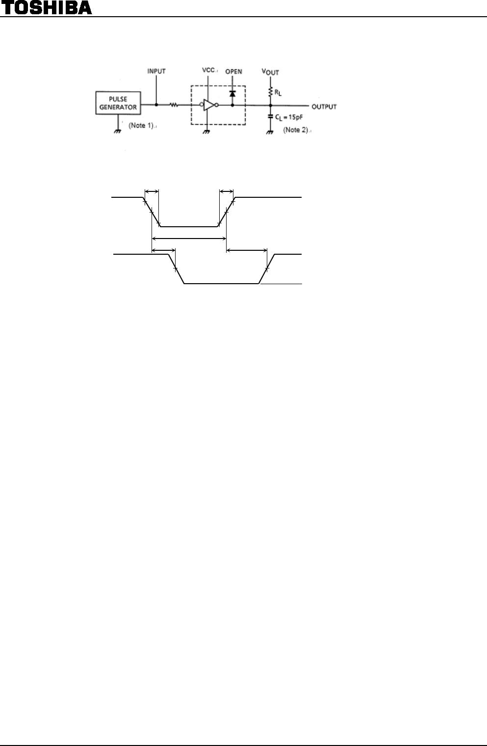
Turn-on delay t
ON
7
V
CC
= 5.0 V, V
OUT
= 50 V
R
L
= 125 Ω
C
L
= 15 pF
― 0.6 ―
μs
Turn-off delay t
OFF
― 0.6 ―