1
COMMERCIAL AND INDUSTRIAL TEMPERATURE RANGES
IDT23S08
3.3V ZERO DELAY CLOCK MULTIPLIER
MAY 2010
2003 Integrated Device Technology, Inc. DSC 6394/10c
COMMERCIAL AND INDUSTRIAL TEMPERATURE RANGES
The IDT logo is a registered trademark of Integrated Device Technology, Inc.
FEATURES:
• Phase-Lock Loop Clock Distribution for Applications ranging
from 10MHz to 133MHz operating frequency
• Distributes one clock input to two banks of four outputs
• Separate output enable for each output bank
• External feedback (FBK) pin is used to synchronize the outputs
to the clock input
• Output Skew <200 ps
• Low jitter <200 ps cycle-to-cycle
• 1x, 2x, 4x output options (see table):
– IDT23S08-1 1x
– IDT23S08-2 1x, 2x
– IDT23S08-3 2x, 4x
– IDT23S08-4 2x
– IDT23S08-1H, -2H, and -5H for High Drive
• No external RC network required
• Operates at 3.3V VDD
• Spread spectrum compatible
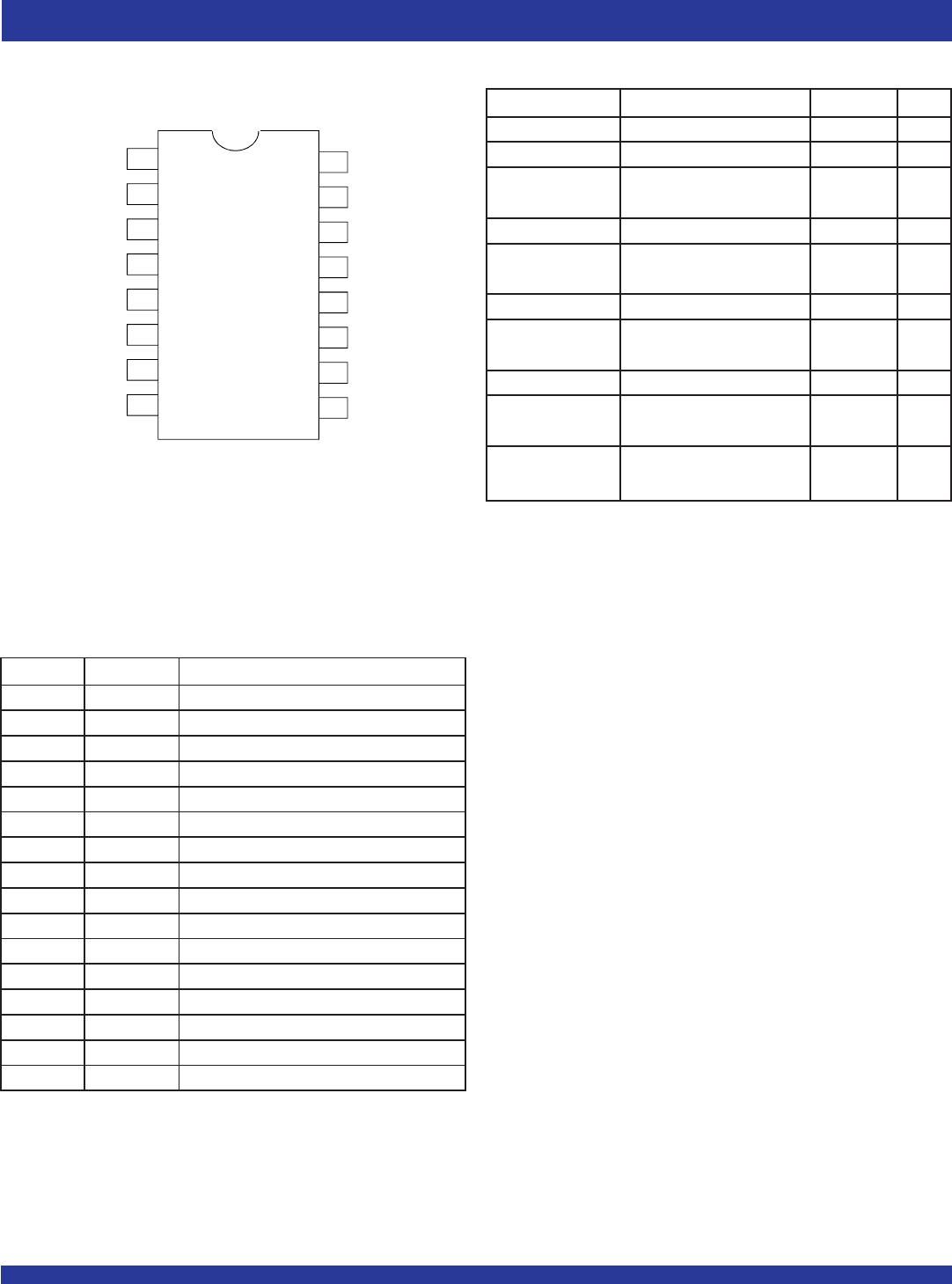
• Available in SOIC and TSSOP packages
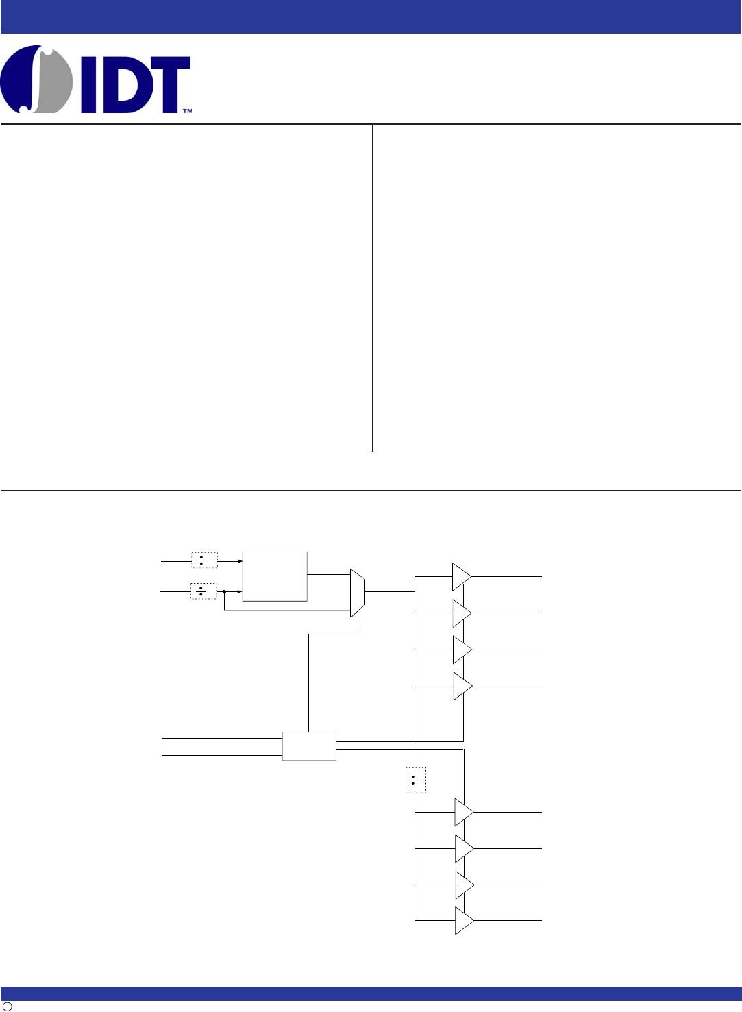
FUNCTIONAL BLOCK DIAGRAM
DESCRIPTION:
The IDT23S08 is a high-speed phase-lock loop (PLL) clock multiplier. It is
designed to address high-speed clock distribution and multiplication applica-
tions. The zero delay is achieved by aligning the phase between the incoming
clock and the output clock, operable within the range of 10 to 133MHz.
The IDT23S08 has two banks of four outputs each that are controlled via two
select addresses. By proper selection of input addresses, both banks can be
put in tri-state mode. In test mode, the PLL is turned off, and the input clock
directly drives the outputs for system testing purposes. In the absence of an
input clock, the IDT23S08 enters power down. In this mode, the device will
draw less than 12µA for Commercial Temperature range and less than 25µA
for Industrial temperature range, and the outputs are tri-stated.
The IDT23S08 is available in six unique configurations for both pre-
scaling and multiplication of the Input REF Clock. (See available options
table.)
The PLL is closed externally to provide more flexibility by allowing the user
to control the delay between the input clock and the outputs.
The IDT23S08 is characterized for both Industrial and Commercial opera-
tion.
IDT23S08
3.3V ZERO DELAY CLOCK
MULTIPLIER, SPREAD
SPECTRUM COMPATIBLE
PLL
S1
2
14
15
3
CLKA1
CLKA2
CLKA3
CLKA4
6
10
11
CLKB1
CLKB2
CLKB3
CLKB4
9
FBK
16
Control
Logic
7
8
1
REF
S2
(-2, -3)
(-3, -4)
(-5)
2
2
2