LTC2941-1
3
29411f
elecTrical characTerisTics
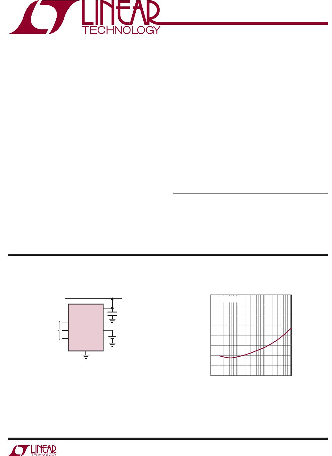
The l denotes the specifications which apply over the full operating
temperature range, otherwise specifications are at T
A
= 25°C. (Note 2)
SYMBOL PARAMETER CONDITIONS MIN TYP MAX UNITS
Digital Inputs and Digital Outputs
V
ITH
Logic Input Threshold, AL/CC, SCL,
SDA
l
0.3 • V
SENSE
+
0.7 • V
SENSE
+
V
V
OL
Low Level Output Voltage, AL/CC, SDA I = 3mA
l
0.4 V
I
IN
Input Leakage, AL/CC, SCL, SDA V
IN
= V
SENSE
+
/2
l
1 µA
C
IN
Input Capacitance, AL/CC, SCL, SDA (Note 7)
l
10 pF
t
PCC
Minimum Charge Complete (CC) Pulse
Width
1 µs
I
2
C Timing Characteristics
f
SCL(MAX)
Maximum SCL Clock Frequency
l
400 900 kHz
t
BUF(MIN)
Bus Free Time Between Stop/Start
l
1.3 µs
t
SU,STA(MIN)
Minimum Repeated Start Setup Time
l
600 ns
t
HD,STA(MIN)
Minimum Hold Time (Repeated)
Start Condition
l
600 ns
t
SU,STO(MIN)
Minimum Setup Time for Stop
Condition
l
600 ns
t
SU,DAT(MIN)
Minimum Data Setup Time Input
l
100 ns
t
HD,DATI(MIN)
Minimum Data Hold Time Input
l
0 µs
t
HD,DATO
Data Hold Time Output
l
0.3 0.9 µs
t
of
Data Output Fall Time (Notes 6, 7)
l
20 + 0.1 • C
B
300 ns
Note 1: Stresses beyond those listed under Absolute Maximum Ratings
may cause permanent damage to the device. Exposure to any Absolute
Maximum Rating condition for extended periods may affect device
reliability and lifetime.
Note 2: All currents into pins are positive, all voltages are referenced to
GND unless otherwise specified
Note 3: I
SUPPLY
= I
SENSE
+
+ I
SENSE
–
Note 4: The equivalent charge of an LSB in the accumulated charge
registers (C,D) depends on the setting of the internal pre-scaling factor M.
It is calculated by:
See Choosing Coulomb Counter Prescaler M section for more information.
1mAh = 3.6A • s = 3.6C (Coulomb), 0.085mAh = 306mC.
Note 5: Deviation of q
LSB
from its nominal value. Data is for a new device
and does not include long-term sense resistor aging. See the Internal
Sense Resistor section for more information.
Note 6: C
B
= capacitance of one bus line in pF (10pF ≤ C
B
≤ 400pF).
Note 7: Guaranteed by design, not subject to test.
Note 8: Value decreases if exposed pad is soldered to large copper area.
See Power Dissipation section for more information.
Timing Diagram
t
SU, DAT
t
SU, STO
t
SU, STA
t
BUF
t
HD, STA
t
HD, DATO,
t
HD, DATI
t
HD, STA
START
CONDITION
STOP
CONDITION
REPEATED START
CONDITION
START
CONDITION
SDA
SCL
29411 F01
t
of
Figure 1. Definition of Timing on I
2
C Bus