AD820
Rev. H | Page 15 of 24
00873-034
AD820
+
+V
S
R
L
100pF
0.01µF
V
OUT
V
IN
3
2
4
7
6
+
Figure 33. Unity-Gain Follower, Used for Figure 34
00873-037
100
90
10
0%
10mV s
GND
Figure 34. V
S
= 5 V, 0 V; Unity-Gain Follower Response to 40 mV Step
Centered 40 mV Above Ground
00873-035
AD820
+
+V
S
R
L
100pF
0.01µF
V
IN
2
3
4
7
6
V
OUT
+
10kΩ 20kΩ
Figure 35. Gain-of-2 Inverter, Used for Figure 36 and Figure 37
00873-036
100
90
10
0%
1V 2µS
GND
Figure 36. V
S
= 5 V, 0 V; Gain-of-2 Inverter Response to 2.5 V Step,
Centered −1.25 V Below Ground
00873-038
100
90
10
0%
10mV s
GND
Figure 37. V
S
= 5 V, 0 V; Gain-of-2 Inverter Response to 20 mV Step, Centered
20 mV Below Ground
AD820
Rev. H | Page 16 of 24
APPLICATIONS INFORMATION
INPUT CHARACTERISTICS
In the AD820, N-channel JFETs are used to provide a low offset,
low noise, high impedance input stage. Minimum input common-
mode voltage extends from 0.2 V below –V
S
to 1 V less than
+V
S
. Driving the input voltage closer to the positive rail causes a
loss of amplifier bandwidth (as can be seen by comparing the
large signal responses shown in Figure 29 and Figure 32) and
increased common-mode voltage error, as illustrated in
Figure 20.
The AD820 does not exhibit phase reversal for input voltages
up to and including +V
S
. Figure 38a shows the response of an
AD820 voltage follower to a 0 V to 5 V (+V
S
) square wave input.
The input and output are superimposed. The output polarity
tracks the input polarity up to +V
S
with no phase reversal. The
reduced bandwidth above a 4 V input causes the rounding of
the output waveform. For input voltages greater than +V
S
, a
resistor in series with the AD820 positive input prevents phase
reversal, at the expense of greater input voltage noise. This is
illustrated in Figure 38b.
Because the input stage uses N-channel JFETs, input current
during normal operation is negative; the current flows out from
the input terminals. If the input voltage is driven more positive
than +V
S
0.4 V, the input current reverses direction as internal
device junctions become forward biased. This is illustrated in
Figure 7.
A current-limiting resistor should be used in series with the
input of the AD820 if there is a possibility of the input voltage
exceeding the positive supply by more than 300 mV, or if an
input voltage is applied to the AD820 when ±V
S
= 0 V. The
amplifier can be damaged if left in that condition for more than
10 seconds. A 1 kΩ resistor allows the amplifier to withstand up
to 10 V of continuous overvoltage, and increases the input
voltage noise by a negligible amount.
Input voltages less than −V
S
are a completely different story.
The amplifier can safely withstand input voltages 20 V below
the negative supply voltage as long as the total voltage from
the positive supply to the input terminal is less than 36 V. In
addition, the input stage typically maintains picoamp level
input currents across that input voltage range.
The AD820 is designed for 13 nV/√Hz wideband input voltage
noise and maintains low noise performance to low frequencies
(refer to Figure 14). This noise performance, along with the
AD820 low input current and current noise, means that the
AD820 contributes negligible noise for applications with source
resistances greater than 10 kΩ and signal bandwidths greater
than 1 kHz. This is illustrated in Figure 39.
00873-039
100
90
10
0%
1V
1V
1V
10µs
GND
+V
S
100
90
10
0%
1V
1V
2µs
GND
AD820
+
5V
R
P
V
OUT
+
V
IN
+
(b)
(a)
Figure 38. (a) Response with R
P
= 0 Ω; V
IN
from 0 V to +V
S
(b) V
IN
= 0 V to +V
S
+ 200 mV,
V
OUT
= 0 V to +V
S
, R
P
= 49.9 kΩ
100k
0.1
10k 10G
SOURCE IMPEDANCE (Ω)
INPUT VOLTAGE NOISE (µV rms)
00873-040
10k
1k
100
10
1
100k 1M 10M 100M 1G
WHENEVER JOHNSON NOISE IS GREATER THAN
AMPLIFIER NOISE, AMPLIFIER NOISE CAN BE
CONSIDERED NEGLIGIBLE FOR APPLICATION.
RESISTOR JOHNSON
NOISE
1kHz
10Hz
AMPLIFIER-GENERATED
NOISE
Figure 39. Total Noise vs. Source Impedance
AD820
Rev. H | Page 17 of 24
OUTPUT CHARACTERISTICS
The AD820 unique bipolar rail-to-rail output stage swings
within 5 mV of the negative supply and 10 mV of the positive
supply with no external resistive load. The approximate output
saturation resistance of the AD820 is 40 Ω sourcing and 20 Ω
sinking. This can be used to estimate output saturation voltage
when driving heavier current loads. For instance, when sourcing
5 mA, the saturation voltage to the positive supply rail is 200 mV;
when sinking 5 mA, the saturation voltage to the negative rail
is 100 mV.
The open-loop gain characteristic of the amplifier changes
as a function of resistive load, as shown in Figure 10 through
Figure 13. For load resistances over 20 kΩ, the AD820 input
error voltage is virtually unchanged until the output voltage is
driven to 180 mV of either supply.
If the AD820 output is driven hard against the output saturation
voltage, it recovers within 2 μs of the input returning to the
linear operating region of the amplifier.
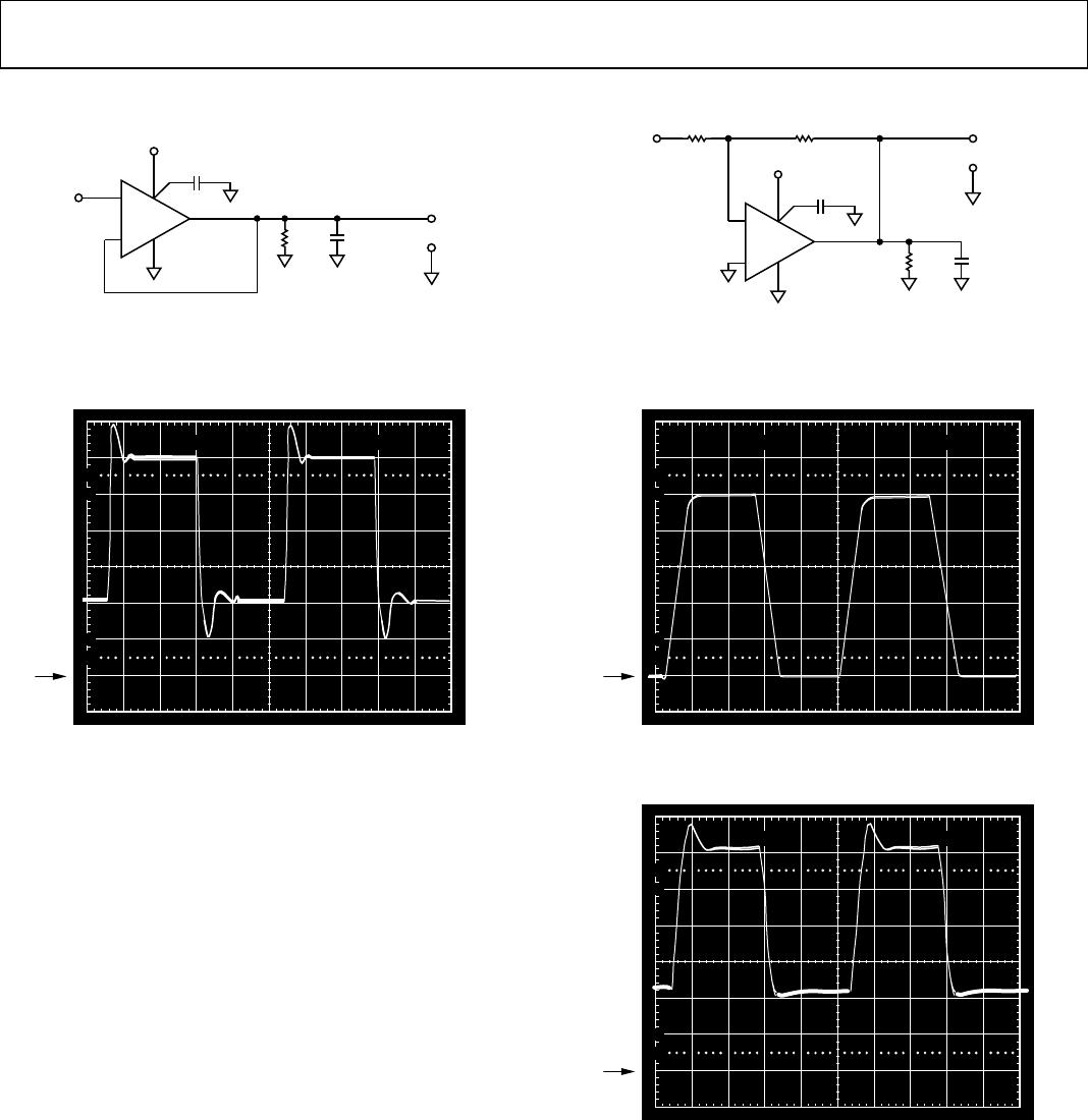
Direct capacitive load interacts with the effective output imped-
ance of the amplifier to form an additional pole in the amplifier
feedback loop, which can cause excessive peaking on the pulse
response or loss of stability. The worst case occurs when the
amplifier is used as a unity-gain follower. Figure 40 shows
AD820 pulse response as a unity-gain follower driving 350 pF.
This amount of overshoot indicates approximately 20 degrees
of phase margin—the system is stable, but is nearing the edge.
Configurations with less loop gain, and as a result less loop
bandwidth, are much less sensitive to capacitance load effects.
Figure 41 is a plot of noise gain vs. the capacitive load that results
in a 20 degree phase margin for the AD820. Noise gain is the
inverse of the feedback attenuation factor provided by the
feedback network in use.
00873-041
20mV 2µs
100
90
10
0%
Figure 40. Small Signal Response of AD820 as Unity-Gain Follower Driving
350 pF Capacitive Load
00873-042
5
1
300 30k
CAPACITIVE LOAD FOR 20º PHASE MARGIN (pF)
NOISE GAIN (1+ )
P
I
P
F
4
3
2
1k 3k 10k
+
R
F
R1
Figure 41. Noise Gain vs. Capacitive Load Tolerance
Figure 42 shows a possible configuration for extending
capacitance load drive capability for a unity-gain follower. With
these component values, the circuit drives 5000 pF with a 10%
overshoot.
0
0873-043
AD820
+
+
+
V
S
–V
S
0.01µF
0.01µF
20pF
20k
100
V
OUT
V
IN
3
2
4
7
6
+
Figure 42. Extending Unity-Gain Follower Capacitive Load Capability
Beyond 350 pF
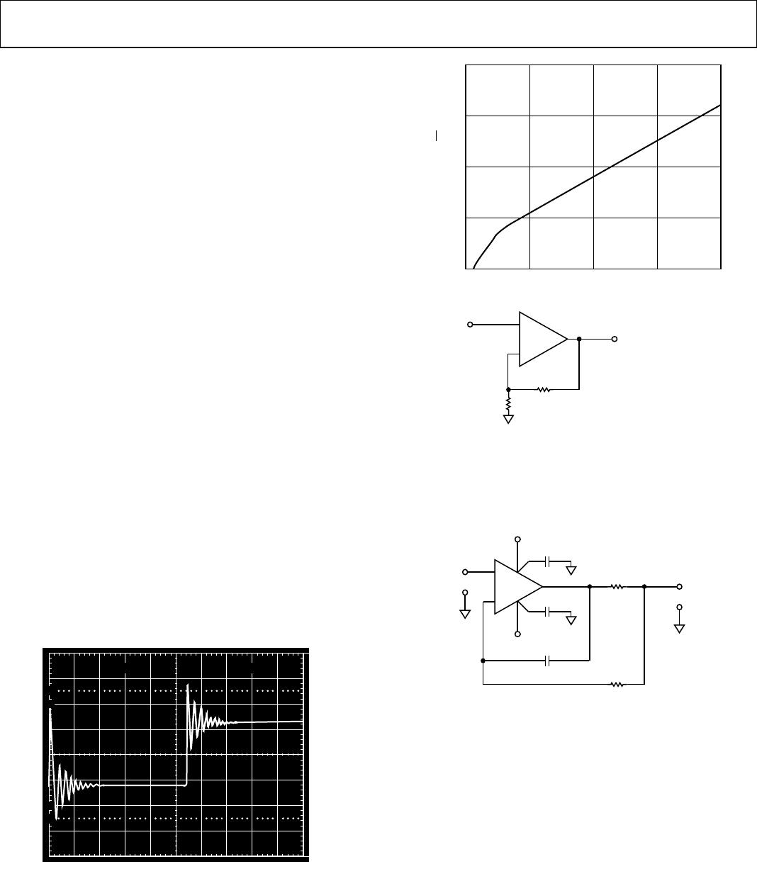
SINGLE-SUPPLY HALF-WAVE AND FULL-WAVE
RECTIFIERS
An AD820 configured as a unity-gain follower and operated
with a single supply can be used as a simple half-wave rectifier.
The AD820 inputs maintain picoamp level input currents even
when driven well below the negative supply. The rectifier puts
that behavior to good use, maintaining an input impedance of
over 10
11
Ω for input voltages from 1 V from the positive supply
to 20 V below the negative supply.
The full- and half-wave rectifier shown in Figure 43 operates as
follows: when V
IN
is above ground, R1 is bootstrapped through
the unity-gain follower, A1, and the loop of Amplifier A2. This
forces the inputs of A2 to be equal; thus, no current flows through
R1 or R2, and the circuit output tracks the input. When V
IN
is
below ground, the output of A1 is forced to ground. The

AD820BRZ-REEL7

Mfr. #:
Manufacturer:
Analog Devices Inc.
Description:
Precision Amplifiers SGL-Supply RR Lo Pwr FET-Inpt
Lifecycle:
New from this manufacturer.
Delivery:
DHL FedEx Ups TNT EMS
Payment:
T/T Paypal Visa MoneyGram Western Union