©2011 Silicon Storage Technology, Inc. S725081A 10/11
17
1 Mbit SPI Serial Flash
SST25VF010A
Data Sheet
Microchip Technology Company
Write-Status-Register (WRSR)
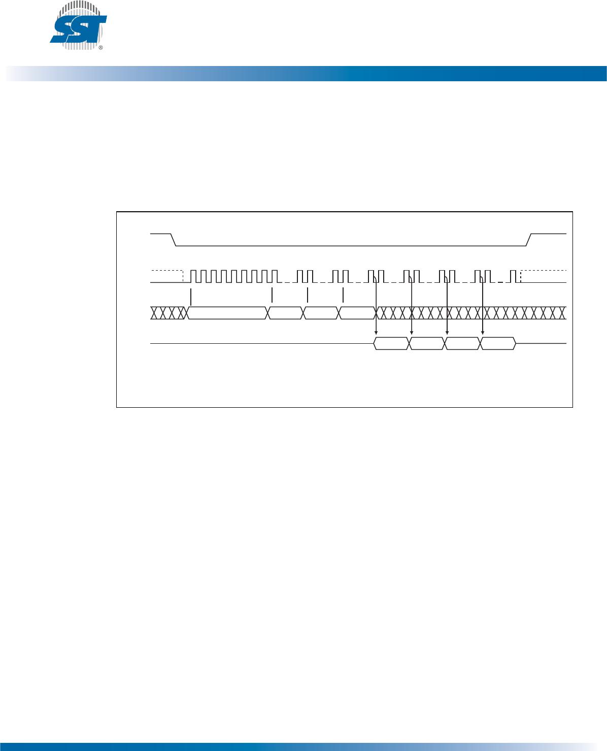
The Write-Status-Register instruction works in conjunction with the Enable-Write-Status-Register
(EWSR) instruction to write new values to the BP1, BP0, and BPL bits of the status register. The Write-
Status-Register instruction must be executed immediately after the execution of the Enable-Write-Sta-
tus-Register instruction (very next instruction bus cycle). This two-step instruction sequence of the
EWSR instruction followed by the WRSR instruction works like SDP (software data protection) com-
mand structure which prevents any accidental alteration of the status register values. The Write-Sta-
tus-Register instruction will be ignored when WP# is low and BPL bit is set to “1”. When the WP# is
low, the BPL bit can only be set from “0” to “1” to lock-down the status register, but cannot be reset
from “1” to “0”. When WP# is high, the lock-down function of the BPL bit is disabled and the BPL, BP0,
and BP1 bits in the status register can all be changed. As long as BPL bit is set to 0 or WP# pin is
driven high (V
IH
) prior to the low-to-high transition of the CE# pin at the end of the WRSR instruction,
the BP0, BP1, and BPL bit in the status register can all be altered by the WRSR instruction. In this
case, a single WRSR instruction can set the BPL bit to “1” to lock down the status register as well as
altering the BP0 and BP1 bit at the same time. See Table 3 for a summary description of WP# and BPL
functions. CE# must be driven low before the command sequence of the WRSR instruction is entered
and driven high before the WRSR instruction is executed. See Figure 14 for EWSR and WRSR instruc-
tion sequences.
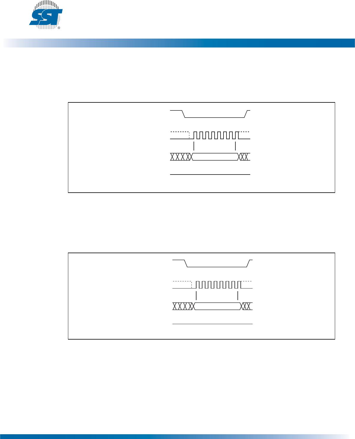
Figure 14:Enable-Write-Status-Register (EWSR) and Write-Status-Register (WRSR)
Sequence
1265 F14.0
MODE 3
HIGH IMPEDANCE
MODE 0
STATUS
REGISTER IN
76543210
MSBMSBMSB
01
MODE 3
SCK
SI
SO
CE#
MODE 0
50
0 1 2 3 4 5 6 7 0 1 2 3 4 5 6 7 8 9 10 11 12 13 14 15