2014 Microchip Technology Inc. DS20005137B-page 13
SST25PF080B
FIGURE 4-12: 64-KBYTE BLOCK-ERASE SEQUENCE
4.5.9 CHIP-ERASE
The Chip-Erase instruction clears all bits in the device
to FFH. A Chip-Erase instruction will be ignored if any
of the memory area is protected. Prior to any Write oper-
ation, the Write-Enable (WREN) instruction must be exe-
cuted. CE# must remain active low for the duration of
the Chip-Erase instruction sequence. The Chip-Erase
instruction is initiated by executing an 8-bit command,
60H or C7H. CE# must be driven high before the instruction
is executed. The user may poll the Busy bit in the software
status register or wait T
CE
for the completion of the
internal self-timed Chip-Erase cycle. See Figure 4-13
for the Chip-Erase sequence.
FIGURE 4-13: CHIP-ERASE SEQUENCE
4.6 Read Security ID
To execute a Read SID operation, the host drives CE#
low, sends the Read Security ID command cycle (88H),
one address cycle, and then one dummy cycle. Each
cycle is eight clock periods long, most significant bit
first.
After the dummy cycle, the device outputs data on the
falling edge of the SCK signal starting from the speci-
fied address location. The data output stream is contin-
uous through all SID addresses until terminated by a
low-to-high transition on CE#. The internal address
pointer automatically increments until the last SID
address is reached, then outputs 00H until CE# goes
high.
4.7 Lockout Security ID
The Lockout SID instruction prevents any future
changes to the Security ID. To execute a Lockout SID,
the host drives CE# low, sends the Lockout SID com-
mand cycle (85H), then drives CE# high. Each cycle is
eight clocks long, most significant bit first. Poll the
BUSY bit in the software status register, or wait T
PSID
,
for the completion of the Lockout SID operation.
CE#
SO
SI
SCK
ADDR
012345678
ADDR ADDR
D8
HIGH IMPEDANCE
15 16
23
24
31
MODE 0
MODE 3
25137 63KBlkEr.0
MSB MSB
CE#
SO
SI
SCK
01234567
60 or C7
HIGH IMPEDANCE
MODE 0
MODE 3
25137 ChEr.0
MSB
SST25PF080B
DS20005137B-page 14 2014 Microchip Technology Inc.
4.8 Program Security ID
The Program SID instruction programs a byte of data in
the user-programmable, Security ID space. Security ID
addresses 08h-1FH are the user-programmable loca-
tions. The device ignores a Program Security ID
instruction pointing to an invalid or protected address,
see Table 4-5. Prior to the program operation, execute
WREN.
To execute a Program SID operation, the host drives
CE# low, sends the Program SID command cycle
(A5H), one address cycle, the data to be programmed,
then drives CE# high. Each cycle is eight clocks long,
most significant bit first. To determine the completion of
the internal, self-timed Program SID operation, poll the
BUSY bit in the software status register, or wait T
PSID
for the completion of the internal self-timed Program
SID operation.
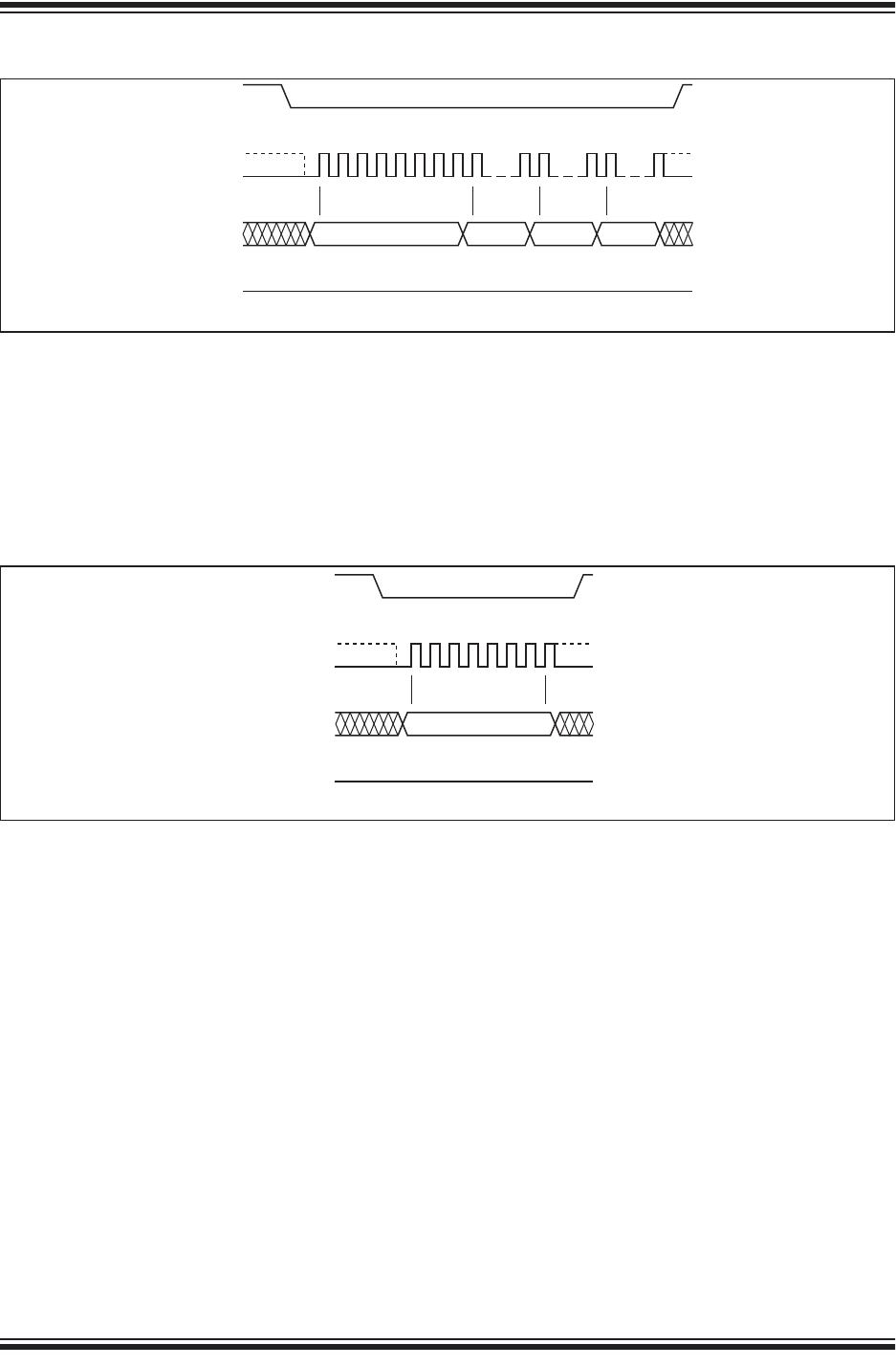
4.8.1 READ-STATUS-REGISTER (RDSR)
The Read-Status-Register (RDSR) instruction allows
reading of the status register. The status register may
be read at any time even during a Write (Program/
Erase) operation. When a Write operation is in prog-
ress, the Busy bit may be checked before sending any
new commands to assure that the new commands are
properly received by the device. CE# must be driven
low before the RDSR instruction is entered and remain
low until the status data is read. Read-Status-Register
is continuous with ongoing clock cycles until it is termi-
nated by a low to high transition of the CE#. See Figure
4-14 for the RDSR instruction sequence.
FIGURE 4-14: READ-STATUS-REGISTER (RDSR) SEQUENCE
TABLE 4-5: PROGRAM SECURITY ID
Program Security ID Address Range
Pre-Programmed at factory 00H – 07H
User Programmable 08H – 1FH
0 1 2 3 4 5 6 7 8 9 10 11 12 13 14
25137 RDSRseq.0
MODE 3
SCK
SI
SO
CE#
Bit 7 Bit 6 Bit 5 Bit 4 Bit 3 Bit 2 Bit 1 Bit 0
05
MODE 0
HIGH IMPEDANCE
Status
Register Out
MSB
MSB
2014 Microchip Technology Inc. DS20005137B-page 15
SST25PF080B
4.8.2 WRITE-ENABLE (WREN)
The Write-Enable (WREN) instruction sets the Write-
Enable-Latch bit in the Status Register to 1 allowing
Write operations to occur. The WREN instruction must
be executed prior to any Write (Program/Erase) opera-
tion. The WREN instruction may also be used to allow
execution of the Write-Status-Register (WRSR)
instruction; however, the Write-Enable-Latch bit in the
Status Register will be cleared upon the rising edge
CE# of the WRSR instruction. CE# must be driven high
before the WREN instruction is executed.
FIGURE 4-15: WRITE ENABLE (WREN) SEQUENCE
4.8.3 WRITE-DISABLE (WRDI)
The Write-Disable (WRDI) instruction resets the Write-
Enable-Latch bit and AAI bit to 0 disabling any new
Write operations from occurring. The WRDI instruction
will not terminate any programming operation in prog-
ress. Any program operation in progress may continue
up to T
BP
after executing the WRDI instruction. CE#
must be driven high before the WRDI instruction is exe-
cuted.
FIGURE 4-16: WRITE DISABLE (WRDI) SEQUENCE
4.8.4 ENABLE-WRITE-STATUS-
REGISTER (EWSR)
The Enable-Write-Status-Register (EWSR) instruction
arms the Write-Status-Register (WRSR) instruction
and opens the status register for alteration. The Write-
Status-Register instruction must be executed immedi-
ately after the execution of the Enable-Write-Status-
Register instruction. This two-step instruction
sequence of the EWSR instruction followed by the
WRSR instruction works like SDP (software data pro-
tection) command structure which prevents any acci-
dental alteration of the status register values. CE# must
be driven low before the EWSR instruction is entered
and must be driven high before the EWSR instruction
is executed.
CE#
SO
SI
SCK
01234567
06
HIGH IMPEDANCE
MODE 0
MODE 3
25137 WREN.0
MSB
CE#
SO
SI
SCK
01234567
04
HIGH IMPEDANCE
MODE 0
MODE 3
25137 WRDI.0
MSB

SST25PF080B-80-4C-SAE-T

Mfr. #:
Manufacturer:
Microchip Technology
Description:
NOR Flash 2.3V to 3.6V 8Mbit SPI Serial Flash
Lifecycle:
New from this manufacturer.
Delivery:
DHL FedEx Ups TNT EMS
Payment:
T/T Paypal Visa MoneyGram Western Union