2014 Microchip Technology Inc. DS20005137B-page 19
SST25PF080B
5.0 ELECTRICAL SPECIFICATIONS
Absolute Maximum Stress Ratings (Applied conditions greater than those listed under “Absolute Maxi-
mum Stress Ratings” may cause permanent damage to the device. This is a stress rating only and func-
tional operation of the device at these conditions or conditions greater than those defined in the operational
sections of this data sheet is not implied. Exposure to absolute maximum stress rating conditions may
affect device reliability.)
Temperature Under Bias.................................................. -55°C to +125°C
Storage Temperature .................................................... -65°C to +150°C
D. C. Voltage on Any Pin to Ground Potential.................................-0.5V to V
DD
+0.5V
Transient Voltage (<20 ns) on Any Pin to Ground Potential ......................-2.0V to V
DD
+2.0V
Package Power Dissipation Capability (T
A
= 25°C) ...................................... 1.0W
Surface Mount Solder Reflow Temperature ...............................260°C for 10 seconds
Output Short Circuit Current
1
...................................................... 50mA
1. Output shorted for no more than one second. No more than one output shorted at a time.
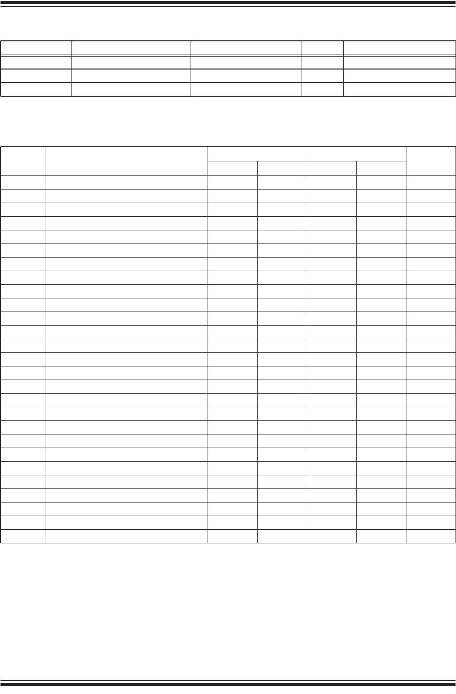
TABLE 5-1: OPERATING RANGE
Range Ambient Temp V
DD
Commercial 0°C to +70°C 2.3-3.6V
TABLE 5-2: AC CONDITIONS OF TEST
1
1. See Figures 5-5 and 5-6
Input Rise/Fall Time Output Load
5ns C
L
=30pF
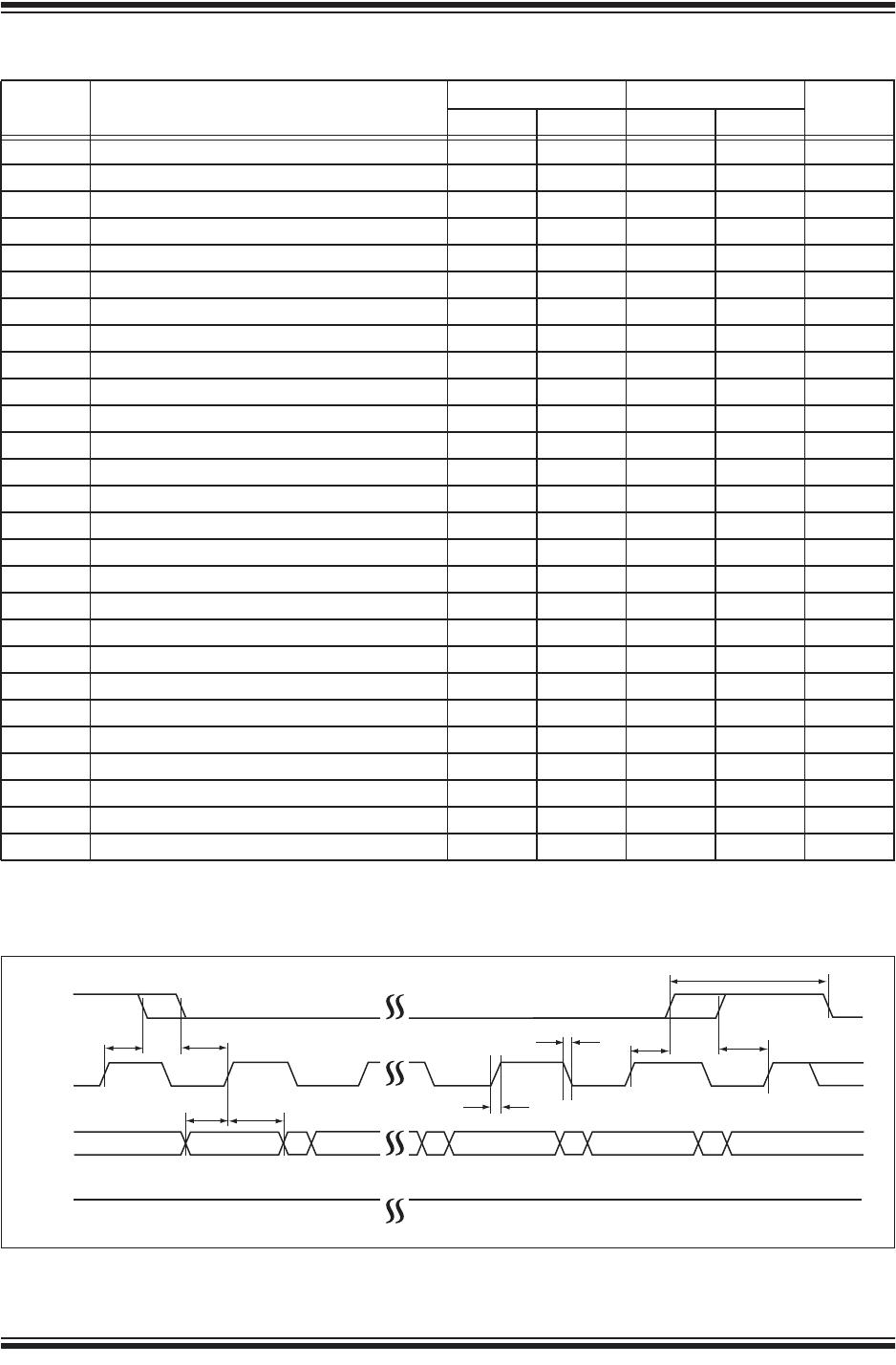
TABLE 5-3: DC OPERATING CHARACTERISTICS
Symbol Parameter
Limits
Test ConditionsMin Max Units
I
DDR
Read Current 12 mA CE#=0.1 V
DD
/0.9 V
DD
@33 MHz, SO=open
I
DDR3
Read Current 20 mA CE#=0.1 V
DD
/0.9 V
DD
@80 MHz, SO=open
I
DDW
Program and Erase Current 30 mA CE#=V
DD
I
SB
Standby Current 20 µA CE#=V
DD
, V
IN
=V
DD
or V
SS
I
LI
Input Leakage Current 1µAV
IN
=GND to V
DD
, V
DD
=V
DD
Max
I
LO
Output Leakage Current 1µAV
OUT
=GND to V
DD
, V
DD
=V
DD
Max
V
IL
Input Low Voltage 0.7 V V
DD
=V
DD
Min
V
IH
Input High Voltage 0.7 V
DD
V V
DD
=V
DD
Max
V
OL
Output Low Voltage 0.2 V I
OL
=100 μA, V
DD
=V
DD
Min
V
OL2
Output Low Voltage 0.4 V I
OL
=1.6 mA, V
DD
=V
DD
Min
V
OH
Output High Voltage V
DD
-0.2 V I
OH
=-100 μA, V
DD
=V
DD
Min
TABLE 5-4: CAPACITANCE (T
A
= 25°C, F=1 MHZ, OTHER PINS OPEN)
Parameter Description Test Condition Maximum
C
OUT
1
1. This parameter is measured only for initial qualification and after a design or process change that could affect this parameter.
Output Pin Capacitance V
OUT
=0V 12pF
C
IN
1
Input Capacitance V
IN
=0V 6pF