© Semiconductor Components Industries, LLC, 2016
September, 2016 − Rev. 20
1 Publication Order Number:
MJD44H11/D
MJD44H11(NPN),
MJD45H11(PNP)
Complementary Power
Transistors
DPAK for Surface Mount Applications
Designed for general purpose power and switching such as output or
driver stages in applications such as switching regulators, converters,
and power amplifiers.
Features
• Lead Formed for Surface Mount Application in Plastic Sleeves
(No Suffix)
• Straight Lead Version in Plastic Sleeves (“−1” Suffix)
• Electrically Similar to Popular D44H/D45H Series
• Low Collector Emitter Saturation Voltage
• Fast Switching Speeds
• Complementary Pairs Simplifies Designs
• Epoxy Meets UL 94 V−0 @ 0.125 in
• NJV Prefix for Automotive and Other Applications Requiring
Unique Site and Control Change Requirements; AEC−Q101
Qualified and PPAP Capable
• These Devices are Pb−Free, Halogen Free/BFR Free and are RoHS
Compliant
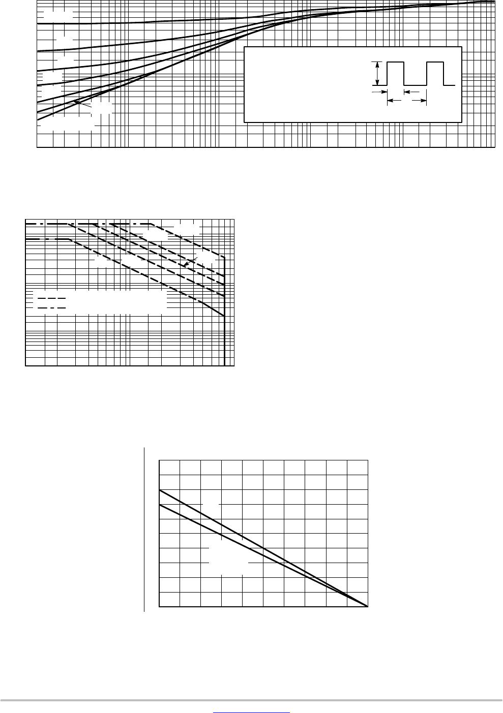
MAXIMUM RATINGS (T
A
= 25_C, common for NPN and PNP, minus
sign, “−”, for PNP omitted, unless otherwise noted)
Rating Symbol Max Unit
Collector−Emitter Voltage V
CEO
80 Vdc
Emitter−Base Voltage V
EB
5 Vdc
Collector Current − Continuous I
C
8 Adc
Collector Current − Peak I
CM
16 Adc
Total Power Dissipation
@ T
C
= 25°C
Derate above 25°C
P
D
20
0.16
W
W/°C
Total Power Dissipation (Note 1)
@ T
A
= 25°C
Derate above 25°C
P
D
1.75
0.014
W
W/°C
Operating and Storage Junction
Temperature Range
T
J
, T
stg
−55 to +150 °C
ESD − Human Body Model HBM 3B V
ESD − Machine Model MM C V
Stresses exceeding those listed in the Maximum Ratings table may damage the
device. If any of these limits are exceeded, device functionality should not be
assumed, damage may occur and reliability may be affected.
1. These ratings are applicable when surface mounted on the minimum pad
sizes recommended.
SILICON
POWER TRANSISTORS
8 AMPERES
80 VOLTS, 20 WATTS
IPAK
CASE 369D
STYLE 1
DPAK
CASE 369C
STYLE 1
MARKING DIAGRAMS
A = Assembly Location
Y = Year
WW = Work Week
J4xH11 = Device Code
x = 4 or 5
G = Pb−Free Package
1
2
3
4
AYWW
J4
xH11G
See detailed ordering and shipping information in the package
dimensions section on page 7 of this data sheet.
ORDERING INFORMATION
1
2
3
4
AYWW
J4
xH11G
www.onsemi.com
IPAKDPAK
COMPLEMENTARY
1
BASE
3
EMITTER
COLLECTOR
2, 4
1
BASE
3
EMITTER
COLLECTOR
2, 4
DPAK
CASE 369G
STYLE 1
1
2
3
4