5
FN3183.5
December 3, 2015
Detailed Description
As shown in the Functional Diagram, the ICL7673 includes a
comparator which senses the input voltages V
P
and V
S
. The
output of the comparator drives the first inverter and the
open-drain N-Channel transistor P
BAR
. The first inverter
drives a large P-Channel switch, P
1
, a second inverter, and
another open-drain N-Channel transistor, S
BAR
. The second
inverter drives another large P-Channel switch P
2
. The
ICL7673, connected to a main and a backup power supply,
will connect the supply of greater potential to its output. The
circuit provides break-before-make switch action as it
switches from main to backup power in the event of a main
power supply failure. For proper operation, inputs V
P
and V
S
must not be allowed to float, and, the difference in the two
supplies must be greater than 50mV. The leakage current
through the reverse biased parasitic diode of switch P
2
is
very low.
Output Voltage
The output operating voltage range is 2.5V to 15V. The
insertion loss between either input and the output is a
function of load current, input voltage, and temperature. This
is due to the P-Channels being operated in their triode
region, and, the ON-resistance of the switches is a function
of output voltage V
O
. The ON-resistance of the P-Channels
have positive temperature coefficients, and therefore as
temperature increases the insertion loss also increases. At
low load currents the output voltage is nearly equal to the
greater of the two inputs. The maximum voltage drop across
switch P
1
or P
2
is 0.5V, since above this voltage the body-
drain parasitic diode will become forward biased. Complete
switching of the inputs and open-drain outputs typically
occurs in 50s.
Input Voltage
The input operating voltage range for V
P
or V
S
is 2.5V to
15V. The input supply voltage (V
P
or V
S
) slew rate should be
limited to 2V per microsecond to avoid potential harm to the
circuit. In line-operated systems, the rate-of-rise (or fall) of
the supply is a function of power supply design. For battery
applications it may be necessary to use a capacitor between
the input and ground pins to limit the rate-of-rise of the
supply voltage. A low-impedance capacitor such as a
0.047F disc ceramic can be used to reduce the rate-of-rise.
Status Indicator Outputs
The N-Channel open drain output transistors can be used to
indicate which supply is connected, or can be used to drive
external PNP transistors to increase the power switching
capability of the circuit. When using external PNP power
transistors, the output current is limited by the beta and
thermal characteristics of the power transistors. The
application section details the use of external PNP
transistors.
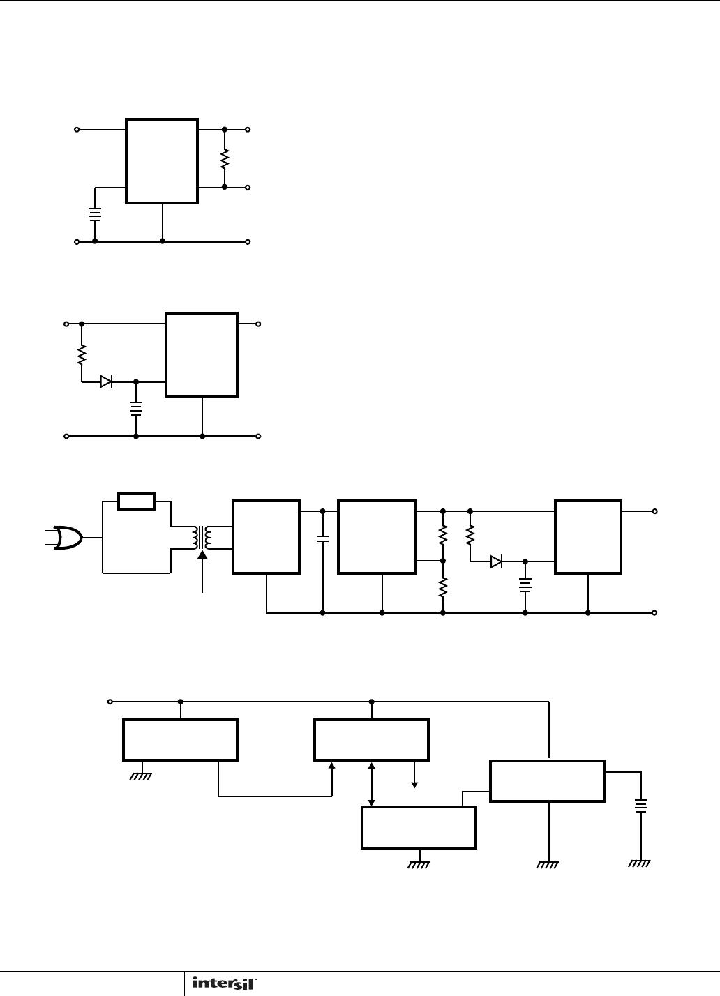
Applications
A typical discrete battery backup circuit is illustrated in Figure
6. This approach requires several components, substantial
printed circuit board space, and high labor cost. It also
consumes a fairly high quiescent current. The ICL7673
battery backup circuit, illustrated in Figure 7, will often replace
such discrete designs and offer much better performance,
higher reliability, and lower system manufacturing cost. A
trickle charge system could be implemented with an additional
resistor and diode as shown in Figure 8. A complete low
power AC to regulated DC system can be implemented using
the ICL7673 and ICL7663S micropower voltage regulator as
shown in Figure 9.
I
S
LEAKAGE CURRENT
INPUT V
P
(V)
02456 81012
1mA
100mA
10nA
1nA
1000pA
10pA
1pA
I
LOAD
= 10mA
V
S
= 0V
85°C
25°C
FIGURE 5. I
S
LEAKAGE CURRENT V
P
TO V
S
AS A
FUNCTION OF INPUT VOLTAGE
+5V
PRIMARY
DC POWER
GND
NiCAD
BATTERY
STACK
V
O
+5V OR
+3V
STATUS
INDICATOR
FIGURE 6. DISCRETE BATTERY BACKUP CIRCUIT
ICL7673