PMLL4148L,115

PMLL4148L_PMLL4448 All information provided in this document is subject to legal disclaimers. © NXP B.V. 2011. All rights reserved.
Product data sheet Rev. 8 — 1 February 2011 3 of 11
NXP Semiconductors
PMLL4148L; PMLL4448
High-speed switching diodes
[1] Device mounted on an FR4 PCB, single-sided copper, tin-plated and standard footprint.
[2] T
j
=25°C prior to surge.
6. Thermal characteristics
[1] Device mounted on an FR4 PCB, single-sided copper, tin-plated and standard footprint.
7. Characteristics
[1] When switched from I
F
= 10 mA to I
R
=60mA; R
L
= 100 Ω; measured at I
R
=1mA.
[2] When switched from I
F
=50mA; t
r
=20ns.
P
tot
total power dissipation T
amb
=25°C
[1]
- 500 mW
T
j
junction temperature - 200 °C
T
amb
ambient temperature 65 +200 °C
T
stg
storage temperature 65 +200 °C
Table 6. Limiting values …continued
In accordance with the Absolute Maximum Rating System (IEC 60134).
Symbol Parameter Conditions Min Max Unit
Table 7. Thermal characteristics
Symbol Parameter Conditions Min Typ Max Unit
R
th(j-a)
thermal resistance from
junction to ambient
in free air
[1]
- - 350 K/W
R
th(j-sp)
thermal resistance from
junction to solder point
- - 300 K/W
Table 8. Characteristics
T
amb
=25
°
C unless otherwise specified.
Symbol Parameter Conditions Min Typ Max Unit
V
F
forward voltage
PMLL4148L I
F
=50mA --1V
PMLL4448 I
F
=5mA 620- 720mV
I
F
=100mA --1V
I
R
reverse current V
R
=20V --25nA
V
R
=20V; T
j
=150°C --50μA
I
R
reverse current
PMLL4448 V
R
=20V; T
j
=100°C --3μA
C
d
diode capacitance V
R
=0V; f=1MHz --4pF
t
rr
reverse recovery time
[1]
--4ns
V
FR
forward recovery voltage
[2]
--2.5V
PMLL4148L_PMLL4448 All information provided in this document is subject to legal disclaimers. © NXP B.V. 2011. All rights reserved.
Product data sheet Rev. 8 — 1 February 2011 4 of 11
NXP Semiconductors
PMLL4148L; PMLL4448
High-speed switching diodes
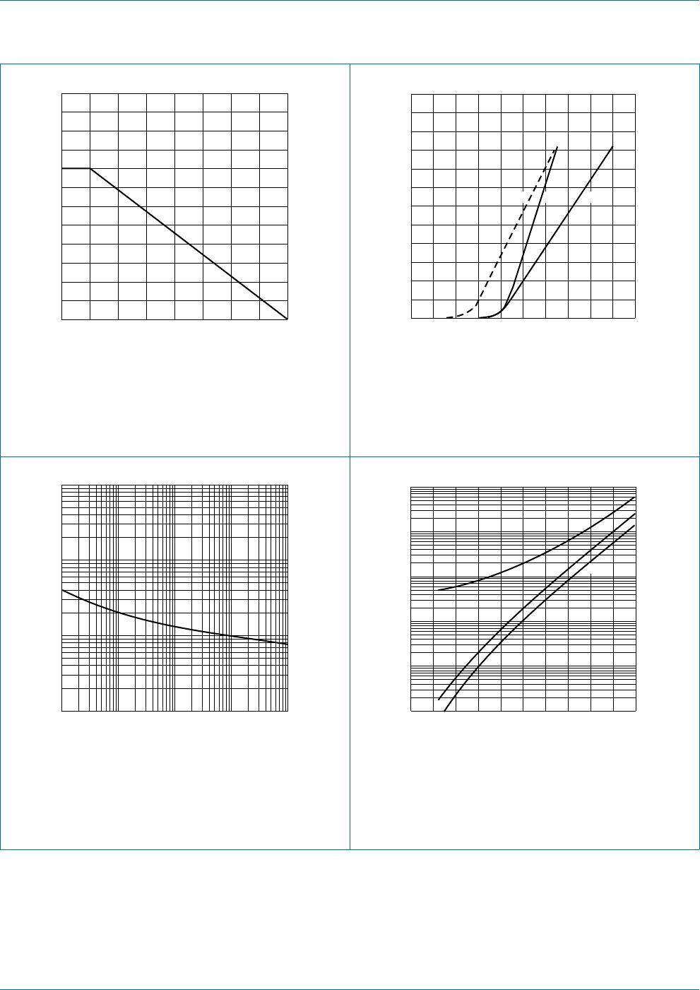
FR4 PCB, standard footprint (1) T
j
= 175 °C; typical values
(2) T
j
=25°C; typical values
(3) T
j
=25°C; maximum values
Fig 1. Forward current as a function of ambient
temperature; derating curve
Fig 2. Forward current as a function of forward
voltage
Based on square wave currents.
T
j
=25°C; prior to surge
(1) V
R
= 75 V; maximum values
(2) V
R
= 75 V; typical values
(3) V
R
= 20 V; typical values
Fig 3. Non-repetitive peak forward current as a
function of pulse duration; maximum values
Fig 4. Reverse current as a function of junction
temperature
0 100 200
300
200
0
100
mbg451
T
amb
(°C)
I
F
(mA)
012
600
0
200
400
mbg464
V
F
(V)
I
F
(mA)
(1) (2) (3)
mbg704
10
1
10
2
I
FSM
(A)
10
1
t
p
(μs)
110
4
10
3
10 10
2
0 100
T
j
(°C)
200
10
3
10
2
10
1
10
2
10
(1) (2)
1
I
R
(μA)
mgd006
(3)
PMLL4148L_PMLL4448 All information provided in this document is subject to legal disclaimers. © NXP B.V. 2011. All rights reserved.
Product data sheet Rev. 8 — 1 February 2011 5 of 11
NXP Semiconductors
PMLL4148L; PMLL4448
High-speed switching diodes
8. Test information
f=1MHz; T
j
=25°C
Fig 5. Diode capacitance as a function of reverse voltage; typical values
01020
1.2
1.0
0.6
0.4
0.8
mgd004
V
R
(V)
C
d
(pF)
(1) I
R
=1mA
Input signal: reverse pulse rise time t
r
= 0.6 ns; reverse voltage pulse duration t
p
= 100 ns; duty cycle δ≤0.05
Oscilloscope: rise time t
r
=0.35ns
Fig 6. Reverse recovery time test circuit and waveforms
Input signal: forward pulse rise time t
r
= 20 ns; forward current pulse duration t
p
100 ns; duty cycle δ≤0.005
Fig 7. Forward recovery voltage test circuit and waveforms
t
rr
(1)
+ I
F
t
output signal
t
r
t
p
t
10 %
90 %
V
R
input signal
V = V
R
+
I
F
×
R
S
R
S
= 50 Ω
I
F
D.U.T.
R
i
= 50 Ω
SAMPLING
OSCILLOSCOPE
mga881
t
r
t
t
p
10 %
90 %
I
input signal
R
S
= 50 Ω
I
R
i
= 50 Ω
OSCILLOSCOPE
1 kΩ 450 Ω
D.U.T.
mga88
2
V
FR
t
output signal
V

PMLL4148L,115

Mfr. #:
Manufacturer:
Nexperia
Description:
Diodes - General Purpose, Power, Switching SW GPP 75V 200MA
Lifecycle:
New from this manufacturer.
Delivery:
DHL FedEx Ups TNT EMS
Payment:
T/T Paypal Visa MoneyGram Western Union

Products related to this Datasheet