TJA1057 All information provided in this document is subject to legal disclaimers. © NXP Semiconductors N.V. 2017. All rights reserved.
Product data sheet Rev. 6 — 24 August 2017 4 of 25
NXP Semiconductors
TJA1057
High-speed CAN transceiver
6. Pinning information
6.1 Pinning
6.2 Pin description
[1] HVSON8 package die supply ground is connected to both the GND pin and the exposed center pad. The
GND pin must be soldered to board ground. For enhanced thermal and electrical performance, it is
recommended that the exposed center pad also be soldered to board ground.
a. SO8 b. SO8 with V
IO
c. HVSON8 d. HVSON8 with V
IO
Fig 2. Pin configuration diagrams
7-$7
7-$*7
7;'
6
*1' &$1+
9
&&
&$1/
5;' QF
DDD
7-$*7
7;'
6
*1' &$1+
9
&&
&$1/
5;'
9
,
2
DDD
5;'
9
&&
*1'
7;'
QF
&$1/
&$1+
6
DDD
7-$*7.
WHUPLQDO
LQGH[DUHD
7UDQVSDUHQWWRSYLHZ
5;'
9
&&
*1'
7;'
9
,
2
&$1/
&$1+
6
DDD
7-$*7.
WHUPLQDO
LQGH[DUHD
7UDQVSDUHQWWRSYLHZ
Table 3. Pin description
Symbol Pin Description
TXD 1 transmit data input
GND
[1]
2 ground
V
CC
3 supply voltage
RXD 4 receive data output; reads out data from the bus lines
n.c. 5 not connected in TJA1057T, TJA1057GT and TJA1057GTK
V
IO
5 supply voltage for I/O level adapter in TJA1057GT/3 and TJA1057GTK/3
CANL 6 LOW-level CAN bus line
CANH 7 HIGH-level CAN bus line
S 8 Silent mode control input
TJA1057 All information provided in this document is subject to legal disclaimers. © NXP Semiconductors N.V. 2017. All rights reserved.
Product data sheet Rev. 6 — 24 August 2017 5 of 25
NXP Semiconductors
TJA1057
High-speed CAN transceiver
7. Functional description
7.1 Operating modes
The TJA1057 supports two operating modes, Normal and Silent. The operating mode is
selected via pin S. See Table 4
for a description of the operating modes under normal
supply conditions.
[1] ‘x’ = don’t care.
7.1.1 Normal mode
A LOW level on pin S selects Normal mode. In this mode, the transceiver can transmit and
receive data via the bus lines, CANH and CANL (see Figure 1
for the block diagram). The
differential receiver converts the analog data on the bus lines into digital data which is
output on pin RXD. The slopes of the output signals on the bus lines are controlled
internally and are optimized in a way that guarantees the lowest possible EME.
7.1.2 Silent mode
A HIGH level on pin S selects Silent mode. The transmitter is disabled in Silent mode,
releasing the bus pins to recessive state. All other IC functions, including the receiver,
continue to operate as in Normal mode. Silent mode can be used to prevent a faulty CAN
controller disrupting all network communications.
7.2 Fail-safe features
7.2.1 TXD dominant time-out function
A 'TXD dominant time-out' timer is started when pin TXD is set LOW. If the LOW state on
this pin persists for longer than t
to(dom)TXD
, the transmitter is disabled, releasing the bus
lines to recessive state. This function prevents a hardware and/or software application
failure from driving the bus lines to a permanent dominant state (blocking all network
communications). The TXD dominant time-out timer is reset when pin TXD is set HIGH.
The TXD dominant time-out time also defines the minimum possible bit rate of
approximately 25 kbit/s.
7.2.2 Internal biasing of TXD and S input pins
Pins TXD and S have internal pull-ups to V
CC
(or V
IO
in TJA1057GT(K)/3 variants) to
ensure a safe, defined state in case one or both of these pins are left floating. Pull-up
currents flow in these pins in all states; both pins should be held HIGH in Silent mode to
minimize supply current.
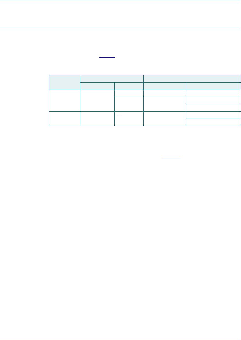
Table 4. Operating modes
Mode Inputs Outputs
Pin S Pin TXD CAN driver Pin RXD
Normal LOW LOW dominant LOW
HIGH recessive LOW when bus dominant
HIGH when bus recessive
Silent HIGH x
[1]
biased to recessive LOW when bus dominant
HIGH when bus recessive
TJA1057 All information provided in this document is subject to legal disclaimers. © NXP Semiconductors N.V. 2017. All rights reserved.
Product data sheet Rev. 6 — 24 August 2017 6 of 25
NXP Semiconductors
TJA1057
High-speed CAN transceiver
7.2.3 Undervoltage detection on pins V
CC
and V
IO
(TJA1057GT(K)/3)
If V
CC
or V
IO
drops below the undervoltage detection level, V
uvd(VCC)
/V
uvd(VIO)
, the
transceiver switches off and disengages from the bus (zero load; bus pins floating) until
the supply voltage has recovered. The output drivers are enabled once both V
CC
and V
IO
are again within their operating ranges and TXD has been reset to HIGH.
7.2.4 Overtemperature protection
The output drivers are protected against overtemperature conditions. If the virtual junction
temperature exceeds the shutdown junction temperature, T
j(sd)
, both output drivers are
disabled. When the virtual junction temperature drops below T
j(sd)
again, the output
drivers recover once TXD has been reset to HIGH (waiting for TXD to go HIGH prevents
output driver oscillation due to small variations in temperature).
7.2.5 V
IO
supply pin (TJA1057x/3 variants)
Pin V
IO
should be connected to the microcontroller supply voltage (see Figure 6). The
signal levels on pins TXD, RXD and S will then be adjusted to the I/O levels of the
microcontroller, allowing for direct interfacing without additional glue logic.
For versions of the TJA1057 without a V
IO
pin, the V
IO
input is internally connected to V
CC
.
The signal levels of pins TXD, RXD and S are set to levels compatible with 5 V
microcontrollers.

TJA1057T/1Z

Mfr. #:
Manufacturer:
NXP Semiconductors
Description:
CAN Interface IC TJA1057T/SO8//1/REEL 13 Q1 NDP SSB
Lifecycle:
New from this manufacturer.
Delivery:
DHL FedEx Ups TNT EMS
Payment:
T/T Paypal Visa MoneyGram Western Union