1
DECEMBER 2016
DSC-6117/15
©
2016 Integrated Device Technology, Inc. All rights reserved. Product specifications subject to change without notice.
3.3 VOLT HIGH-DENSITY SUPERSYNC II™
36-BIT FIFO
65,536 x 36
131,072 x 36
IDT72V36100
IDT72V36110
IDT and the IDT logo are registered trademarks of Integrated Device Technology, Inc. The SuperSync II FIFO is a trademark of Integrated Device Technology, Inc.
COMMERCIAL AND INDUSTRIAL TEMPERATURE RANGES
FEATURES:
••
••
• Choose among the following memory organizations:
IDT72V36100
⎯⎯
⎯⎯
⎯ 65,536 x 36
IDT72V36110
⎯⎯
⎯⎯
⎯ 131,072 x 36
••
••
• Higher density, 2Meg and 4Meg SuperSync II FIFOs
••
••
• Up to 166 MHz Operation of the Clocks
••
••
• User selectable Asynchronous read and/or write ports (PBGA Only)
••
••
• User selectable input and output port bus-sizing
- x36 in to x36 out
- x36 in to x18 out
- x36 in to x9 out
- x18 in to x36 out
- x9 in to x36 out
••
••
• Big-Endian/Little-Endian user selectable byte representation
••
••
• 5V input tolerant
••
••
• Fixed, low first word latency
••
••
• Zero latency retransmit
••
••
• Auto power down minimizes standby power consumption
••
••
• Master Reset clears entire FIFO
••
••
• Partial Reset clears data, but retains programmable settings
••
••
• Empty, Full and Half-Full flags signal FIFO status
••
••
• Programmable Almost-Empty and Almost-Full flags, each flag can
default to one of eight preselected offsets
••
••
•
Selectable synchronous/asynchronous timing modes for Almost-
Empty and Almost-Full flags
••
••
•
Program programmable flags by either serial or parallel means
••
••
•
Select IDT Standard timing (using EF and FF flags) or First Word
Fall Through timing (using OR and IR flags)
••
••
•
Output enable puts data outputs into high impedance state
••
••
•
Easily expandable in depth and width
••
••
•
JTAG port, provided for Boundary Scan function (PBGA Only)
••
••
•
Independent Read and Write Clocks (permit reading and writing
simultaneously)
••
••
•
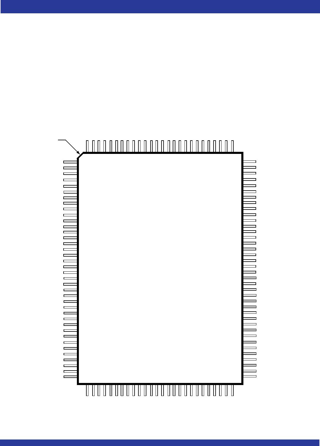
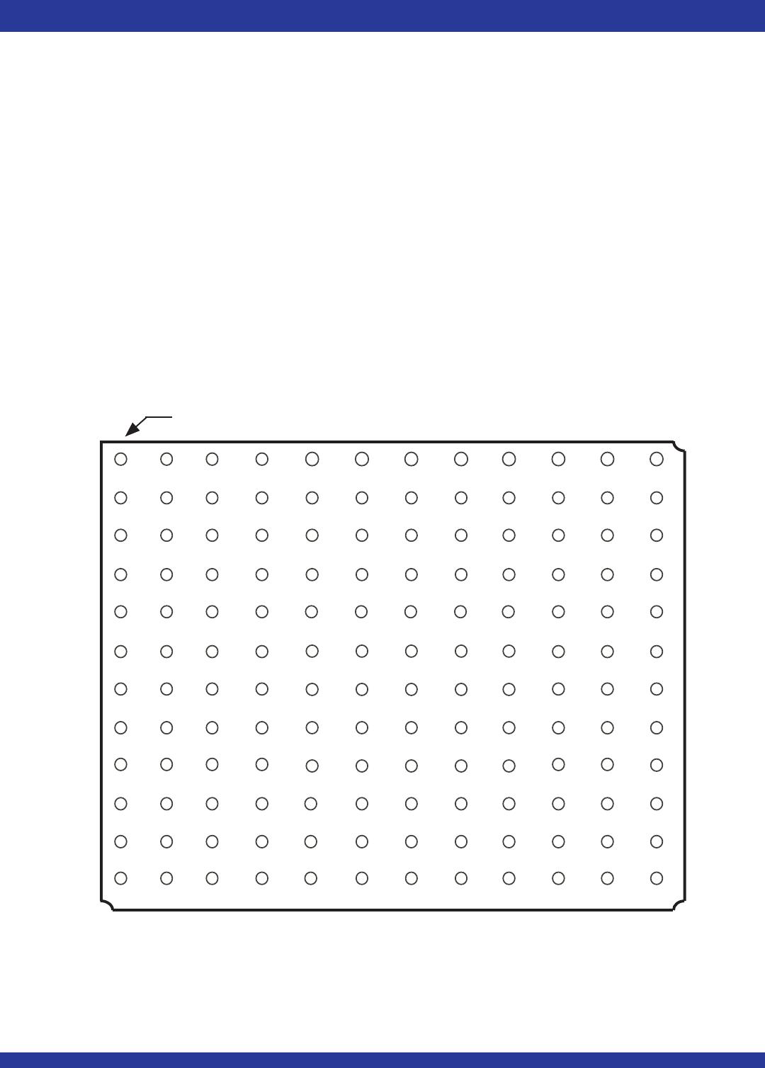
Available in a 128-pin Thin Quad Flat Pack (TQFP) or a 144-pin Plastic
Ball Grid Array (PBGA) (with additional features)
••
••
• Pin compatible to the SuperSync II (IDT72V3640/72V3650/72V3660/
72V3670/72V3680/72V3690) family
••
••
• High-performance submicron CMOS technology
••
••
• Industrial temperature range (–40
°°
°°
°C to +85
°°
°°
°C) is available
••
••
• Green parts available, see ordering information
FUNCTIONAL BLOCK DIAGRAM
INPUT REGISTER
OUTPUT REGISTER
RAM ARRAY
65,536 x 36
131,072 x 36
FLAG
LOGIC
FF/IR
PAF
EF/OR
PAE
HF
READ POINTER
READ
CONTROL
LOGIC
WRITE CONTROL
LOGIC
WRITE POINTER
RESET
LOGIC
WEN
WCLK/WR
D
0
-D
n
(x36, x18 or x9)
LD
MRS
REN
RCLK/RD
OE
Q
0
-Q
n
(x36, x18 or x9)
OFFSET REGISTER
PRS
FWFT/SI
SEN
RT
6117 drw01
BUS
CONFIGURATION
BM
CONTROL
LOGIC
BE
OW
IP
PFM
FSEL0
FSEL1
IW
RM
ASYR
ASYW
JTAG CONTROL
(BOUNDARY
SCAN)
TCK
TMS
TDO
TDI
TRST
*
*
*
*
*
*
*
*
*
*
*Available on the PBGA package only.