8
LTC2051/LTC2052
20512fd
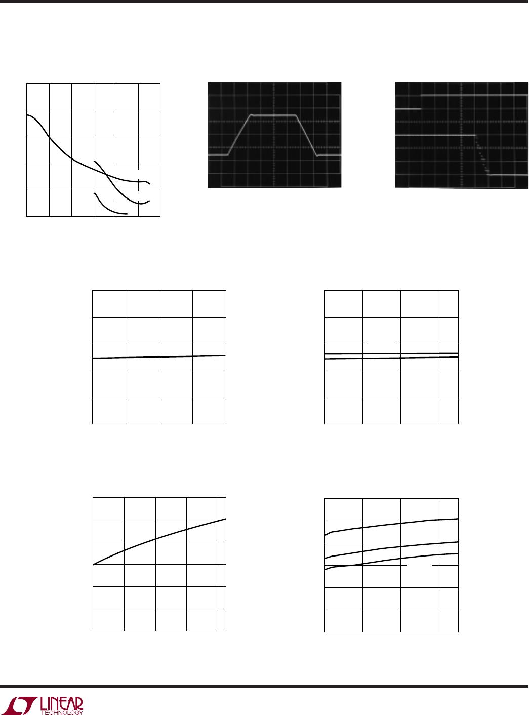
The dual chopper op amp buffers the inputs of A1 and
corrects its offset voltage and offset voltage drift. With the
RC values shown, the power-up warm-up time is typically
20 seconds. The step response of the composite amplifier
does not present settling tails. The LT
®
1677 should be
used when extremely low noise, V
OS
and V
OS
drift are
needed and the input source resistance is low. (For in-
stance a 350Ω strain gauge bridge.) The LT1012 or
equivalent should be used when low bias current (100pA)
is also required in conjunction with DC to 10Hz low noise,
low V
OS
and V
OS
drift. The measured typical input offset
voltages are less than 1μV.
APPLICATIO S I FOR ATIO
WUUU
Shutdown
The LTC2051 includes a shutdown pin in the 10-lead
MSOP. When this active low pin is high or allowed to float,
the device operates normally. When the shutdown pin is
pulled low, the device enters shutdown mode; supply
current drops to 3μA, all clocking stops and the output
assumes a high impedance state.
Clock Feedthrough, Input Bias Current
The LTC2051/LTC2052 use autozeroing circuitry to achieve
an almost zero DC offset over temperature, common
mode voltage and power supply voltage. The frequency of
the clock used for autozeroing is typically 7.5kHz. The
term clock feedthrough is broadly used to indicate visibil-
ity of this clock frequency in the op amp output spectrum.
There are typically two types of clock feedthrough in
autozeroed op amps like the LTC2051/LTC2052.
The first form of clock feedthough is caused by the settling
of the internal sampling capacitor and is input referred;
that is, it is multiplied by the closed-loop gain of the op
amp. This form of clock feedthrough is independent of the
magnitude of the input source resistance or the magnitude
of the gain setting resistors. The LTC2051/LTC2052 have
a residue clock feedthrough of less than 1μV
RMS
input
referred at 7.5kHz.
The second form of clock feedthrough is caused by the
small amount of charge injection occurring during the
sampling and holding of the op amps input offset voltage.
The current spikes are multiplied by the impedance seen
at the input terminals of the op amp, appearing at the
output multiplied by the closed-loop gain of the op amp.
To reduce this form of clock feedthrough, use smaller
valued gain setting resistors and minimize the source
resistance at the input. If the resistance seen at the inputs
is less than 10k, this form of clock feedthrough is less
than 1μV
RMS
input referred at 7.5kHz, or less than the
amount of residue clock feedthrough from the first form
previously described.
Placing a capacitor across the feedback resistor reduces
either form of clock feedthrough by limiting the bandwidth
of the closed-loop gain.
Input bias current is defined as the DC current into the
input pins of the op amp. The same current spikes that
cause the second form of clock feedthrough
previously
described
, when averaged, dominate the DC input bias
current of the op amp below 70°C.
At temperatures above 70°C, the leakage of the ESD
protection diodes on the inputs increase the input bias
currents of both inputs in the positive direction, while the
current caused by the charge injection stays relatively
constant. At elevated temperatures (above 85°C) the
leakage current begins to dominate and both the negative
and positive pin’s input bias currents are in the positive
direction (into the pins).
Input Pins, ESD Sensitivity
ESD voltages above 700V on the input pins of the op amp
will cause the input bias currents to increase (more DC
current into the pins). At these voltages, it is possible to
damage the device to a point where the input bias current
exceeds the maximums specified in this data sheet.
TYPICAL APPLICATIO
U