5
LTC2051/LTC2052
20512fd
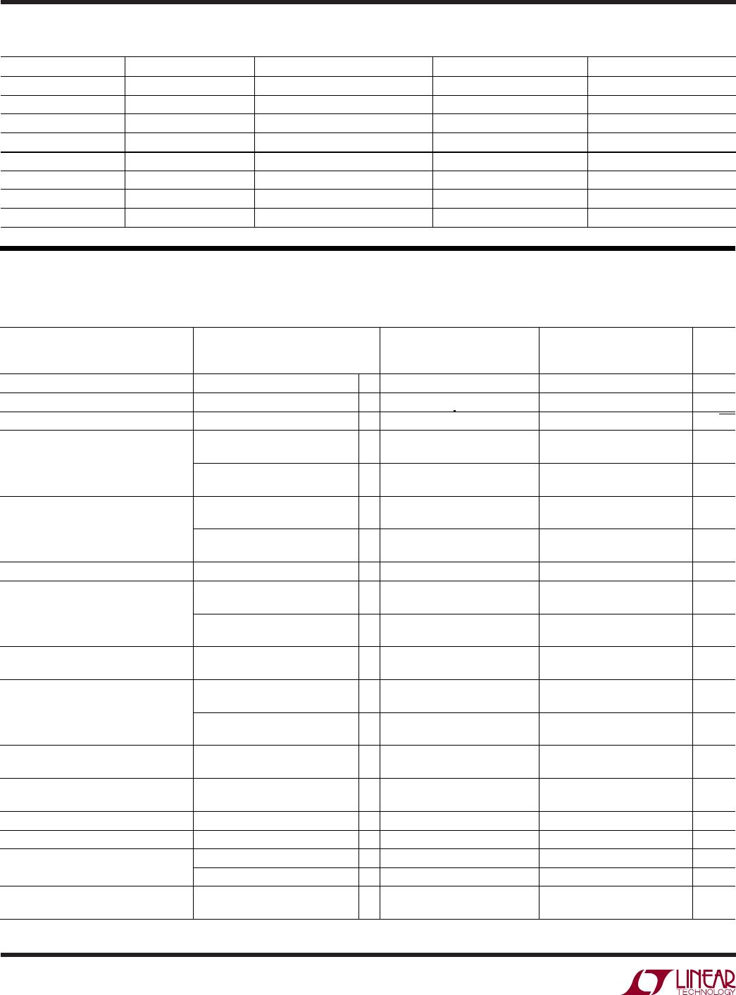
ELECTRICAL CHARACTERISTICS
LTC2051C/LTC2052C
LTC2051I/LTC2052I LTC2051H/LTC2052H
PARAMETER CONDITIONS MIN TYP MAX MIN TYP MAX UNITS
(LTC2051/LTC2052, LTC2051HV/LTC2052HV) The ● denotes the
specifications which apply over the full operating temperature range, otherwise specifications are at T
A
= 25°C. V
S
= 3V, 5V
unless otherwise noted. (Note 3)
Shutdown Pin Input Low Voltage (V
IL
) ● V
–
+ 0.5 V
–
+ 0.5 V
Shutdown Pin Input High Voltage (V
IH
) ● V
+
– 0.5 V
+
– 0.5 V
Shutdown Pin Input Current V
SHDN
= V
IL
, V
S
= 3V ● –1 –3 –1 –3 μA
V
SHDN
= V
IL
, V
S
= 5V ● –2 –5 –2 –5 μA
Internal Sampling Frequency 7.5 7.5 kHz
LTC2051C/LTC2052C
LTC2051I/LTC2052I LTC2051H/LTC2052H
PARAMETER CONDITIONS MIN TYP MAX MIN TYP MAX UNITS
Input Offset Voltage (Note 2) ±1 ±3 ±1 ±3 μV
Average Input Offset Drift (Note 2) ● 0.01 ±0.03 0.01 ±0.05 μV/°C
Long-Term Offset Drift 50 50 nV/√mo
Input Bias Current (Note 4) ±90 ±150 ±90 ±150 pA
● ±300 ±3000 pA
Input Offset Current (Note 4) ±300 ±300 pA
● ±500 ±700 pA
Input Noise Voltage R
S
= 100Ω, DC to 10Hz 1.5 1.5 μV
P-P
Common Mode Rejection Ratio V
CM
= V
–
to V
+
– 1.3 125 130 125 130 dB
● 120 130 120 130 dB
Power Supply Rejection Ratio 120 130 120 130 dB
● 115 130 115 130 dB
Large-Signal Voltage Gain R
L
= 10k 125 140 125 140 dB
● 120 140 120 140 dB
Maximum Output Voltage Swing R
L
= 2k to GND ● ±4.75 ±4.92 ±4.50 ±4.92 V
R
L
= 10k to GND ● ±4.90 ±4.98 ±4.85 ±4.98 V
Slew Rate 22V/μs
Gain Bandwidth Product 3 3 MHz
Supply Current (Per Amplifier) No Load, V
SHDN
= V
IH
● 1 1.5 1 1.5 mA
Supply Current, Shutdown V
SHDN
= V
IL
● 15 30 15 30 μA
Shutdown Pin Input Low Voltage (V
IL
) ● V
–
+ 0.5 V
–
+ 0.5 V
Shutdown Pin Input High Voltage (V
IH
) ● V
+
– 0.5 V
+
– 0.5 V
Shutdown Pin Input Current V
SHDN
= V
IL
● –7 –15 –7 –15 μA
Internal Sampling Frequency 7.5 7.5 kHz
Note 1: Stresses beyond those listed under Absolute Maximum Ratings
may cause permanent damage to the device. Exposure to any Absolute
Maximum Rating condition for extended periods may affect device
reliability and lifetime.
Note 2: These parameters are guaranteed by design. Thermocouple effects
preclude measurements of these voltage levels during automated testing.
Note 3: All versions of the LTC2051/LTC2052 are designed, characterized
and expected to meet the extended temperature limits of –40°C and 125°C.
The LTC2051C/LTC2052C/LTC2051HVC/LTC2052HVC are guaranteed to
meet the temperature limits of 0°C and 70°C. The LTC2051I/LTC2052I/
LTC2051HVI/LTC2052HVI are guaranteed to meet temperature limits of –
40°C and 85°C. The LTC2051H/LTC2051HVH and LTC2052H/LTC2052HVH
(LTC2051HV/LTC2052HV) The ● denotes the specifications which apply over the full operating temperature range, otherwise
specifications are at T
A
= 25°C. V
S
= ±5V unless otherwise noted. (Note 3)
are guaranteed to meet the temperature limits of –40°C and 125°C.
Note 4: The bias current measurement accuracy depends on the proximity of
the negative supply bypass capacitors to the device under test. Because of
this, only the bias current of channel B (LTC2051) and channels A and B
(LTC2052) are 100% tested to the data sheet specifications. The bias
currents of the remaining channels are 100% tested to relaxed limits,
however, their values are guaranteed by design to meet the data sheet limits.
Note 5: This parameter is guaranteed to meet specified performance
through design and characterization. It has not been tested.
Note 6: The θ
JA
specified for the DD package is with minimal PCB heat
spreading metal. Using expanded metal area on all layers of a board
reduces this value.