LTC1403/LTC1403A
10
1403fc
For more information www.linear.com/LTC1403
applications inFormation
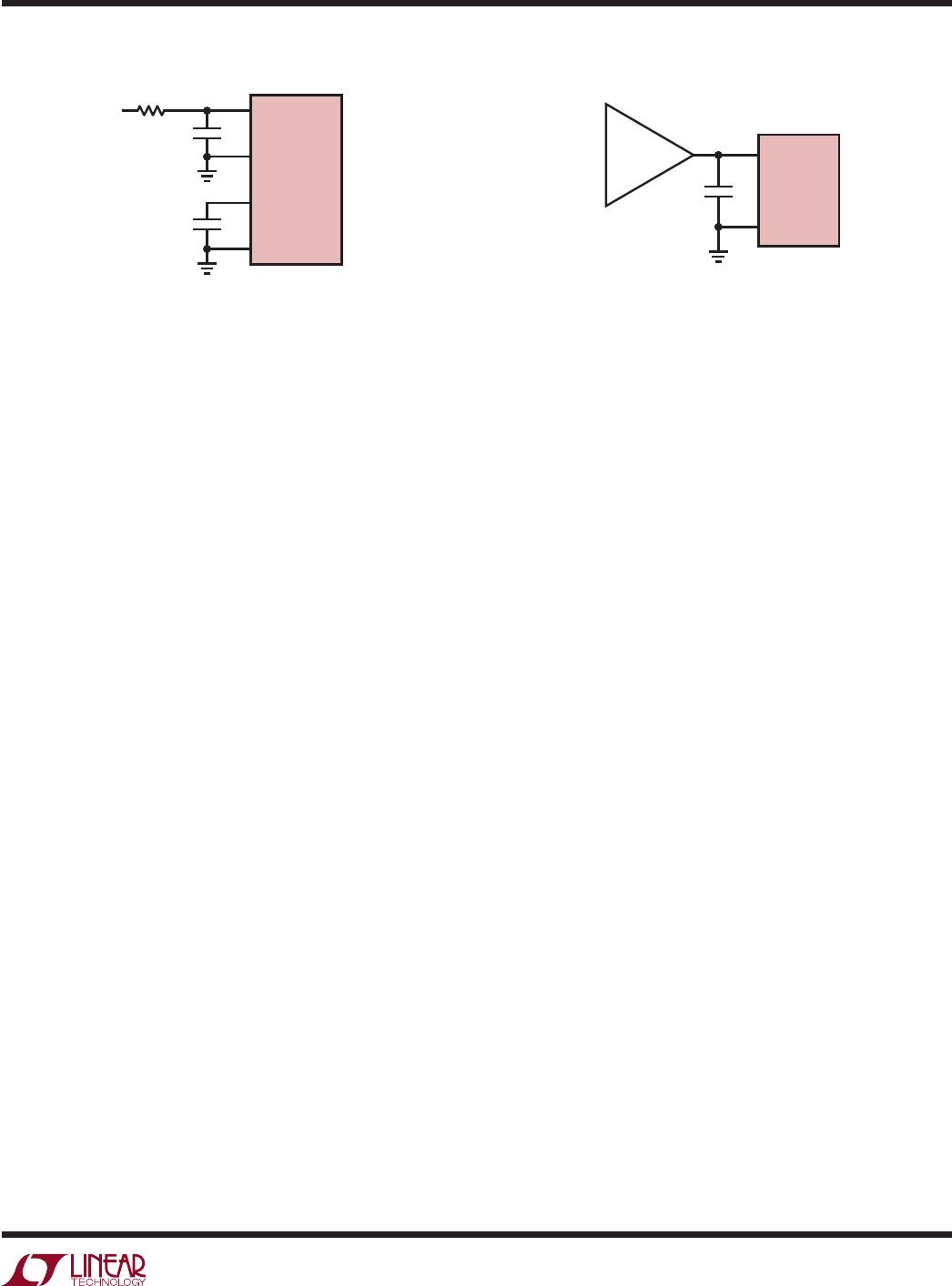
DRIVING THE ANALOG INPUT
The differential analog inputs of the LTC1403/LTC1403A
are easy to drive. The inputs may be driven differentially or
as a single-ended input (i.e., the A
IN
input is grounded).
Both differential analog inputs, A
IN
+
with A
IN
, are sampled
at the same instant. Any unwanted signal that is common
to both inputs of each input pair will be reduced by the
common mode rejection of the sample-and-hold circuit.
The inputs draw only one small current spike while charging
the sample-and-hold capacitors at the end of conversion.
During conversion, the analog inputs draw only a small
leakage current. If the source impedance of the driving
circuit is low, then the LTC1403/LTC1403A inputs can be
driven directly. As source impedance increases, so will
acquisition time. For minimum acquisition time with high
source impedance, a buffer amplifier must be used. The
main requirement is that the amplifier driving the analog
input(s) must settle after the small current spike before
the next conversion starts (settling time must be 39ns
for full throughput rate). Also keep in mind while choos
-
ing an input amplifier, the amount of noise and harmonic
distortion added by the amplifier.
C
HOOSING AN INPUT AMPLIFIER
Choosing an input amplifier is easy if a few requirements
are taken into consideration. First, to limit the magnitude
of the voltage spike seen by the amplifier from charging
the sampling capacitor, choose an amplifier that has a low
output impedance (<100Ω) at the closed-loop bandwidth
frequency. For example, if an amplifier is used in a gain
of 1 and has a unity-gain bandwidth of 50MHz, then the
output impedance at 50MHz must be less than 100Ω. The
second requirement is that the closed-loop bandwidth must
be greater than 40MHz to ensure adequate small-signal
settling for full throughput rate. If slower op amps are
used, more time for settling can be provided by increasing
the time between conversions. The best choice for an op
amp to drive the LTC1403/LTC1403A will depend on the
application. Generally, applications fall into two categories:
AC applications where dynamic specifications are most
critical and time domain applications where DC accuracy
and settling time are most critical. The following list is
a summary of the op amps that are suitable for driving
the LTC1403/LTC1403A. (More detailed information is
available in the Linear Technology Databooks and on the
LinearView
TM
CD-ROM.)
LT C
®
1566-1: Low Noise 2.3MHz Continuous Time Low-
Pass Filter.
LT1630: Dual 30MHz Rail-to-Rail Voltage FB Amplifier.
2.7V to ±15V supplies. Very high A
VOL
, 500µV offset and
520ns settling to 0.5LSB for a 4V swing. THD and noise
are –93dB to 40kHz and below 1LSB to 320kHz (A
V
= 1,
2V
P-P
into 1kΩ, V
S
= 5V), making the part excellent for AC
applications (to 1/3 Nyquist) where rail-to-rail performance
is desired. Quad version is available as LT1631.
LT1632: Dual 45MHz Rail-to-Rail Voltage FB Amplifier.
2.7V to ±15V supplies. Very high A
VOL
, 1.5mV offset and
400ns settling to 0.5LSB for a 4V swing. It is suitable
for applications with a single 5V supply. THD and noise
are –93dB to 40kHz and below 1LSB to 800kHz (A
V
= 1,
2V
P-P
into 1kΩ, V
S
= 5V), making the part excellent for
AC applications where rail-to-rail performance is desired.
Quad version is available as LT1633.
LT1813: Dual 100MHz 750V/µs 3mA Voltage Feedback
Amplifier. 5V to ±5V supplies. Distortion is 86dB to 100kHz
and –77dB to 1MHz with ±5V supplies (2V
P-P
into 500Ω).
Excellent part for fast AC applications with ±5V supplies.
LT1801: 80MHz GBWP, –75dBc at 500kHz, 2mA/Amplifier,
8.5nV/√Hz.
LT1806/LT1807: 325MHz GBWP, –80dBc Distortion at
5MHz, Unity-Gain Stable, R-R In and Out, 10mA/Ampli
-
fier, 3.5nV/√Hz.
LT1810: 180MHz GBWP, 90dBc Distortion at 5MHz, Unity-
Gain Stable, R-R In and Out, 15mA/Amplifier, 16nV/√Hz.
LT1818/LT1819: 400MHz, 2500V/µs,9mA, Single/Dual
Voltage Mode Operational Amplifier.
LT6200: 165MHz GBWP, –85dBc Distortion at 1MHz,
Unity-Gain Stable, R-R In and Out, 15mA/Amplifier,
0.95nV/√Hz.
LT6203: 100MHz
GBWP, 80dBc Distortion at 1MHz, Unity-
Gain Stable, R-R In and Out, 3mA/Amplifier, 1.9nV/√Hz.
LT6600-10: Amplifier/Filter Differential In/Out with 10MHz
Cutoff.
LTC1403/LTC1403A
11
1403fc
For more information www.linear.com/LTC1403
applications inFormation
Figure 1. RC Input Filter
INPUT FILTERING AND SOURCE IMPEDANCE
The noise and the distortion of the input amplifier and other
circuitry must be considered since they will add to the
LTC1403/LTC1403A noise and distortion. The small-signal
bandwidth of the sample-and-hold circuit is 50MHz. Any
noise or distortion products that are present at the analog
inputs will be summed over this entire bandwidth. Noisy
input circuitry should be filtered prior to the analog inputs
to minimize noise. A simple 1-pole RC filter is sufficient for
many applications. For example, Figure 1 shows a 47pF
capacitor from A
IN
+
to ground and a 51Ω source resistor to
limit the input bandwidth to 47MHz. The 47pF capacitor also
acts as a charge reservoir for the input sample-and-hold
and isolates the ADC input from sampling-glitch sensitive
circuitry. High quality capacitors and resistors should be
used since these components can add distortion. NPO
and silvermica type dielectric capacitors have excellent
linearity. Carbon surface mount resistors can generate
distortion from self heating and from damage that may
occur during soldering. Metal film surface mount resistors
are much less susceptible to both problems. When high
amplitude unwanted signals are close in frequency to the
desired signal frequency, a multiple pole filter is required.
High external source resistance, combined with the 13pF of
input capacitance, will reduce the rated 50MHz bandwidth
and increase acquisition time beyond 39ns.
INPUT RANGE
The analog inputs of the LTC1403/LTC1403A may be
driven fully differentially with a single supply. Each input
may swing up to 3V
P-P
individually. In the conversion
range, the noninverting input of each channel is always
up to 2.5V more positive than the inverting input of each
channel. The 0V to 2.5V range is also ideally suited for
single-ended input use with single supply applications. The
common mode range of the inputs extend from ground to
the supply voltage V
DD
. If the difference between the A
IN
+
and A
IN
inputs exceeds 2.5V, the output code will stay
fixed at all ones and if this difference goes below 0V, the
output code will stay fixed at all zeros.
INTERNAL REFERENCE
The LTC1403/LTC1403A has an on-chip, temperature
compensated, bandgap reference that is factory trimmed
near 2.5V to obtain 2.5V input span. The reference amplifier
output V
REF
, (Pin 3) must be bypassed with a capacitor to
ground. The reference amplifier is stable with capacitors
of 1µF or greater. For the best noise performance, a 10µF
ceramic or a 10µF tantalum in parallel with a 0.1µF ceramic
is recommended. The V
REF
pin can be overdriven with an
external reference as shown in Figure 2. The voltage of
the external reference must be higher than the 2.5V of
the class A pull-up output of the internal reference. The
recommended range for an external reference is 2.55V to
V
DD
. An external reference at 2.55V will see a DC quiescent
load of 0.75mA and as much as 3mA during conversion.
Figure 2
GND
LTC1403/
LTC1403A
V
REF
10µF
11
3
3V
REF
1403A F02
10µF
11
3
A
IN
LTC1403/
LTC1403A
A
IN
+
47pF
2
1
51Ω
GND
V
REF
1403A F01
LTC1403/LTC1403A
12
1403fc
For more information www.linear.com/LTC1403
applications inFormation
INPUT SPAN VERSUS REFERENCE VOLTAGE
The differential input range has a unipolar voltage span that
equals the difference between the voltage at the reference
buffer output V
REF
at Pin 3, and the voltage at the ground
(Exposed Pad Ground). The differential input range of
the ADC is 0V to 2.5V when using the internal reference.
The internal ADC is referenced to these two nodes. This
relationship also holds true with an external reference.
DIFFERENTIAL INPUTS
The LTC1403/LTC1403A has a unique differential sample-
and-hold circuit that allows inputs from ground to V
DD
.
The ADC will always convert the unipolar difference of
A
IN
+
A
IN
, independent of the common mode voltage
at the inputs. The common mode rejection holds up at
extremely high frequencies, see Figure 3. The only require-
ment is that both inputs not go below ground or exceed
V
DD
. Integral nonlinearity errors (INL) and differential
nonlinearity errors (DNL) are largely independent of the
common mode voltage. However, the offset error will vary.
The change in offset error is typically less than 0.1% of
the common mode voltage.
Figure 4 shows the ideal input/output characteristics for
the LTC1403/LTC1403A. The code transitions occur mid
-
way between successive integer LSB values (i.e., 0.5LSB,
1.5LSB,
2.5LSB, FS 1.5LSB). The output code is natural
binary with 1LSB = 2.5V/16384 = 153µV for the LTC1403A,
and 1LSB = 2.5V/4096 = 610µV for the LTC1403. The
LTC1403A has 1LSB RMS of random white noise.
Figure 3 Figure 4
CMRR vs Frequency
LTC1403/LTC1403A Transfer
Characteristic
FREQUENCY (Hz)
100
CMRR (dB)
0
–20
–40
–60
–80
–100
–120
1k
10k 100k 1M
1403A F03
10M 100M
INPUT VOLTAGE (V)
UNIPOLAR OUTPUT CODE
1403A F04
111...111
111...110
111...101
000...000
000...001
000...010
FS – 1LSB0

LTC1403AIMSE#PBF

Mfr. #:
Manufacturer:
Analog Devices Inc.
Description:
Analog to Digital Converters - ADC Serial 14-B, 2.8Msps Smpl ADCs w/ SD
Lifecycle:
New from this manufacturer.
Delivery:
DHL FedEx Ups TNT EMS
Payment:
T/T Paypal Visa MoneyGram Western Union