1808-FG-225-RC

Critical Link, LLC MitySOM
www.criticallink.com MitySOM-1808 Processor Card
5-MAR-2014
7 Copyright © 2013, Critical Link LLC
Specifications Subject to Change
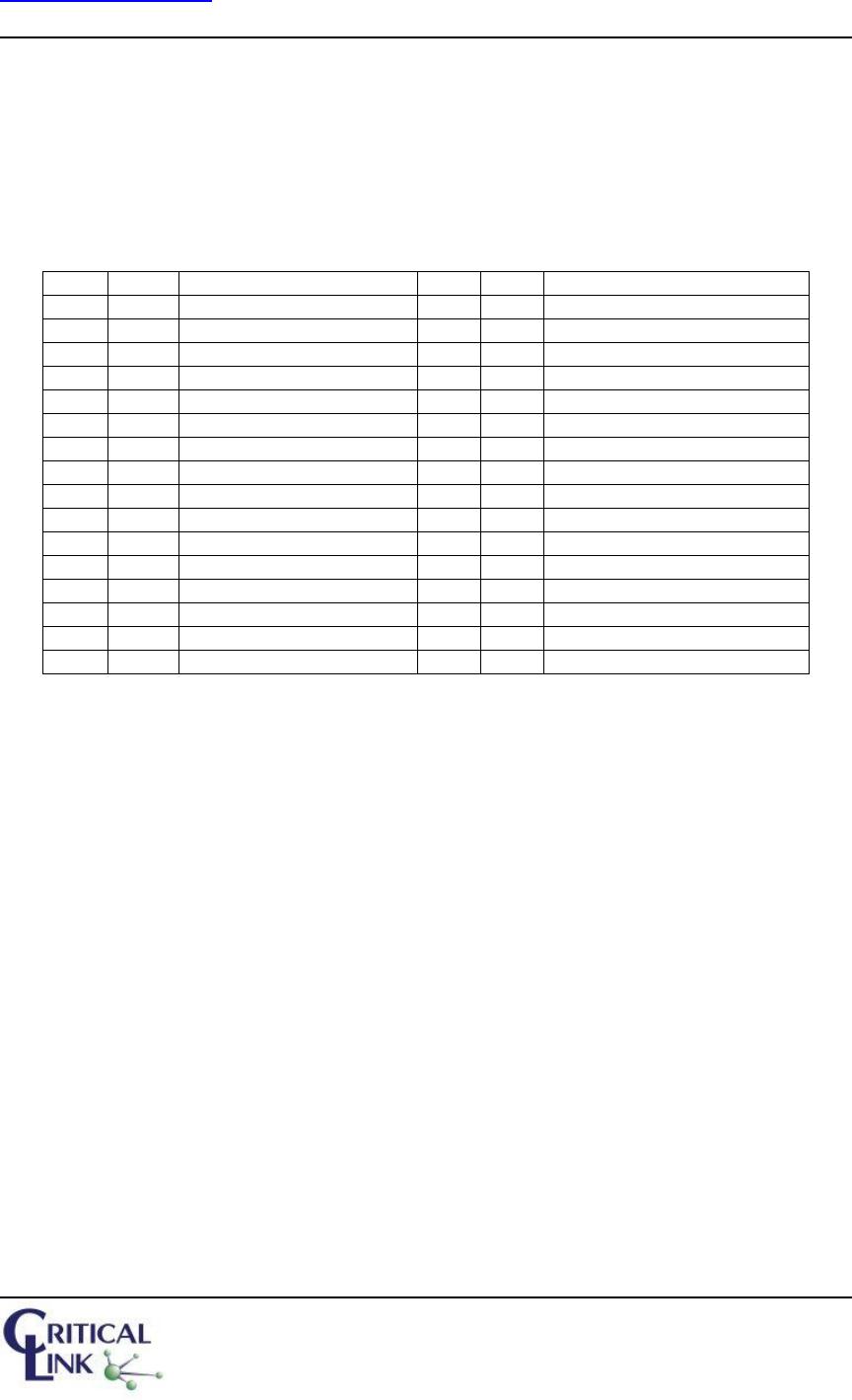
Table 2 Signal Group Description
Signal / Group
Type
Description
3.3 V in
N/A
3.3 volt input power referenced to GND.
EXT_BOOT#
I
Bootstrap configuration pin. Pull low to configure booting
from external UART1.
RESET_IN#
I
Manual Reset. When pulled to GND for a minimum of 1
usec, resets the processor.
SPI1_*
I/O
Serial Peripheral Interface 1 pins.
These pins are direct connects to the corresponding SPI1_*
pins on the AM1808 processor. The SPI1_* function pins are
multiplexed with other functions. These include PWM,
Timers, UARTs, I2C0, and GPIO. For details please refer to
the AM1808 processor specifications.
MII_*
I/O
Media Independent Interface (Ethernet) pins.
These pins are direct connects to the corresponding MII_*
pins on the AM1808 processor. The MII_* function pins are
multiplexed with other functions. These include SPI0, PWM,
Timers, UART0, MCBSP, MCASP, and GPIO. For details
please refer to the AM1808 processor specifications.
MDIO_DAT
MDIO_CLK
I/O
MII/RMII Management Interface pins.
The MDIO_CLK and MDIO_DAT signals are direct connects
to the corresponding MDIO_* signals on the AM1808
processor. The MDIO_* function pins are multiplexed with
other functions. These include SPI0 and Timer functions.
For details please refer to the AM1808 processor
specifications.
GP0_*
I/O
General Purpose / multiplexed pins. These pins are direct
connects to the corresponding GP0[*] pins on the AM1808
processor. The include support for the McASP, general
purpose I/O, UART flow control, and McBSP 1. For details
please refer to the AM1808 processor specifications.
SATA_TX_P
SATA_TX_N
O
Serial ATA Controller Transmit pins.
These pins are direct connects to the corresponding
SATA_TX_* pins on the AM1808 processor. For details
please refer to the AM1808 processor specifications.
SATA_RX_P
SATA_RX_N
I
Serial ATA Controller Receive pins.
These pins are direct connects to the corresponding
SATA_RX_* pins on the AM1808 processor. For details
please refer to the AM1808 processor specifications.
GND
N/A
System Digital Ground.
Critical Link, LLC MitySOM
www.criticallink.com MitySOM-1808 Processor Card
5-MAR-2014
8 Copyright © 2013, Critical Link LLC
Specifications Subject to Change
Signal / Group
Type
Description
EMA_*
I/O
EMIF-A pins. These pins are direct connects to the
corresponding EMA_* pins on the AM1808 processor.
Alternatively, these pins can be configured as GPIOs for
modules that do not have NAND memory present. For details
please refer to the AM1808 processor specifications. Note that
pins 197, 198, 199 and 200 have 1.00K Ohm resistors in
series with the signals on the module.
UPP_*
I/O
Universal Parallel Port pins.
These pins are direct connects to the corresponding UPP_*
pins on the AM1808 processor. The UPP_* function pins are
multiplexed with other functions. These include RMII,
VP_DIN, MMCSD1, and GPIO. For details please refer to
the AM1808 processor specifications.
RMII_*
I/O
Reduced Media Independent Interface pins.
These pins are direct connects to the corresponding RMII_*
pins on the AM1808 processor. The RMII_* function pins
are multiplexed with other functions. These include UPP and
VP_DIN. For details please refer to the AM1808 processor
specifications.
LCD_*
I/O
Liquid Crystal Display pins.
These pins are direct connects to the corresponding LCD_*
pins on the AM1808 processor. The LCD_* function pins are
multiplexed with other functions. These include VP_DOUT,
UPP, MMCSD1, and GPIO. For details please refer to the
AM1808 processor specifications.
VP_*
I/O
Video Port In/Out.
These pins are direct connects to the corresponding VP_* pins
on the AM1808 processor. The VP_* function pins are
multiplexed with other functions. These include UPP,
MMCSD1, and GPIO. For details please refer to the AM1808
processor specifications.
RESET_OUT
I/O
Reset Output pin.
This pin is a direct connect to the RESET_OUT pin on the
AM1808 processor. This pin can also be configured as a
GPIO. For details please refer to the AM1808 processor
specifications.
USB0_*,
USB1_*
I/O
Universal Serial Bus 0 / 1 pins.
These pins are direct connects to the corresponding USB_*
pins on the AM1808 processor. For details please refer to the
AM1808 processor specifications.
Critical Link, LLC MitySOM
www.criticallink.com MitySOM-1808 Processor Card
5-MAR-2014
9 Copyright © 2013, Critical Link LLC
Specifications Subject to Change
DEBUG INTERFACE
Below is the pin-out for the Hirose 31 pin header (DF9-31P-1V(32)) that interfaces with
an available adapter board, CL part number 80-000286, to debug the AM1808.
Debug Interface Connector Description (J2)
Table 3 AM1808 Hirose Connector
Pin
I/O
Signal
Pin
I/O
Signal
1
-
GND
2
O
OMAP EMU1
3
-
GND
4
O
OMAP EMU0
5
-
GND
6
I
OMAP TCK
7
-
GND
8
O
OMAP RTCK
9
-
GND
10
O
OMAP TDO
11
-
GND
12
-
OMAP VCC / 3.3V
13
-
GND
14
I
OMAP TDI
15
-
GND
16
I
OMAP TRST
17
-
GND
18
I
OMAP TMS
19
-
GND
20
-
GND
21
-
GND
22
NC
FPGA VREF / VCCAUX
23
-
GND
24
NC
FPGA TMS
25
-
GND
26
NC
FPGA TCK
27
-
GND
28
NC
FPGA TDO
29
-
GND
30
NC
FPGA TDI
31
-
GND

1808-FG-225-RC

Mfr. #:
Manufacturer:
Critical Link
Description:
System-On-Modules - SOM MitySOM-1808F AM1808 XILINX XC6SLX16
Lifecycle:
New from this manufacturer.
Delivery:
DHL FedEx Ups TNT EMS
Payment:
T/T Paypal Visa MoneyGram Western Union

Products related to this Datasheet