1–4 Chapter 1: Stratix III Device Family Overview
Features Summary
Stratix III Device Handbook, Volume 1 © March 2010 Altera Corporation
Tab le 1 –2 lists the Stratix III FPGA package options and I/O pin counts.
All Stratix III devices support vertical migration within the same package (for
example, you can migrate between the EP3SL50 and EP3SL70 devices in the 780-pin
FineLine BGA package). Vertical migration allows you to migrate to devices whose
dedicated pins, configuration pins, and power pins are the same for a given package
across device densities.
To ensure that a board layout supports migratable densities within one package
offering, enable the applicable vertical migration path within the Quartus
®
II
software. On the Assignments menu, point to Device and click Migration Devices.
You can migrate from the L family to the E family without increasing the number of
LEs available. This minimizes the cost of vertical migration.
Tab le 1 –3 lists the Stratix III FineLine BGA (FBGA) package sizes.
Table 12. Package Options and I/O Pin Counts (Note 1)
Device
484-Pin
FineLine
BGA (2)
780-Pin
FineLine
BGA (2)
1152-Pin
FineLine
BGA (2)
1517-Pin
FineLine BGA
(3)
1760-Pin
FineLine BGA
(3)
EP3SL50 296 488
EP3SL70 296 488
EP3SL110 488 744
EP3SL150 488 744
EP3SL200 488 (5) 744 976 —
EP3SL340 744 (4) 976 1,120
EP3SE50 296 488
EP3SE80 488 744
EP3SE110 488 744
EP3SE260 488 (5) 744 976
Notes to Table 1–2:
(1) The arrows indicate vertical migration.
(2) All I/O pin counts include eight dedicated clock inputs (CLK1p, CLK1n, CLK3p, CLK3n, CLK8p, CLK8n,
CLK10p, and CLK10n) that can be used for data inputs.
(3) All I/O pin counts include eight dedicated clock inputs (CLK1p, CLK1n, CLK3p, CLK3n, CLK8p,
CLK8n, CLK10p, and CLK10n) and eight dedicated corner PLL clock inputs (PLL_L1_CLKp,
PLL_L1_CLKn, PLL_L4_CLKp, PLL_L4_CLKn, PLL_R4_CLKp, PLL_R4_CLKn, PLL_R1_CLKp,
and PLL_R1_CLKn) that can be used for data inputs.
(4) The EP3SL340 FPGA is offered only in the H1152 package, but not offered in the F1152 package.
(5) The EP3SE260 and EP3SL200 FPGAs are offered only in the H780 package, but not offered in the F780 package.
Table 13. FineLine BGA Package Sizes
Dimension 484 Pin 780 Pin 1152 Pin 1517 Pin 1760 Pin
Pitch (mm) 1.00 1.00 1.00 1.00 1.00
Area (mm
2
) 529 841 1,225 1,600 1,849
Length/Width (mmmm) 23/23 29/29 35/35 40/40 43/43
Chapter 1: Stratix III Device Family Overview 1–5
Features Summary
© March 2010 Altera Corporation Stratix III Device Handbook, Volume 1
Tab le 1 –4 lists the Stratix III Hybrid FineLine BGA (HBGA) package sizes.
Stratix III devices are available in up to three speed grades: –2, –3, and –4, with –2
being the fastest. Stratix III devices are offered in both commercial and industrial
temperature range ratings with leaded and lead-free packages. Selectable Core
Voltage is available in specially marked low-voltage devices (L ordering code suffix).
Tab le 1 –5 lists the Stratix III device speed grades.
Table 14. Hybrid FineLine BGA Package Sizes
Dimension 780 Pin 1152 Pin
Pitch (mm) 1.00 1.00
Area (mm
2
) 1,089 1,600
Length/Width (mmmm) 33/33 40/40
Table 15. Speed Grades for Stratix III Devices (Part 1 of 2)
Device
Temperature
Grade
484 -Pin
FineLine
BGA
780-Pin
FineLine
BGA
780-Pin
Hybrid
FineLine
BGA
1152-Pin
FineLine
BGA
1152-Pin
Hybrid
FineLine
BGA
1517-Pin
FineLine
BGA
1760-Pin
FineLine
BGA
EP3SL50
Commercial
–2, –3, –4,
–4L
–2, –3,–4,
–4L
————
Industrial –3, –4, –4L –3, –4, –4L
EP3SL70
Commercial
–2, –3, –4,
–4L
–2, –3, –4,
–4L
————
Industrial –3, –4, –4L –3, –4, –4L
EP3SL110
Commercial
–2, –3, –4,
–4L
–2, –3, –4,
–4L
———
Industrial –3, –4, –4L –3, –4, –4L
EP3SL150
Commercial
–2,–3, –4,
–4L
–2, –3, –4,
–4L
———
Industrial –3, –4, –4L –3, –4, –4L
EP3SL200
Commercial
–2,3, –4,
–4L
–2,–3, –4,
–4L
–2,–3, –4,
–4L
Industrial (1) –3, –4, –4L –3, –4, –4L –3, –4, –4L
EP3SL340
Commercial –2,3, –4 –2, –3, –4 –2, –3, –4
Industrial (1) –3, –4, –4L –3, –4, –4L –3,4, –4L
EP3SE50
Commercial
–2, –3, –4,
–4L
–2, –3, –4,
–4L
————
Industrial –3, –4, –4L –3, –4, –4L
EP3SE80
Commercial
–2, –3, –4,
–4L
–2, –3, –4,
–4L
———
Industrial 3, –4, –4L –3, –4, –4L
EP3SE110
Commercial
–2,–3, –4,
–4L
–2, –3, –4,
–4L
———
Industrial –3, –4, –4L –3, –4, –4L
1–6 Chapter 1: Stratix III Device Family Overview
Architecture Features
Stratix III Device Handbook, Volume 1 © March 2010 Altera Corporation
Architecture Features
The following section describes the various features of the Stratix III family FPGAs.
Logic Array Blocks and Adaptive Logic Modules
The Logic Array Block (LAB) is composed of basic building blocks known as
Adaptive Logic Modules (ALMs) that can be configured to implement logic,
arithmetic, and register functions. Each LAB consists of ten ALMs, carry chains,
shared arithmetic chains, LAB control signals, local interconnect, and register chain
connection lines. ALMs are part of a unique, innovative logic structure that delivers
faster performance, minimizes area, and reduces power consumption. ALMs expand
the traditional 4-input look-up table architecture to 7 inputs, increasing performance
by reducing LEs, logic levels, and associated routing. In addition, ALMs maximize
DSP performance with dedicated functionality to efficiently implement adder trees
and other complex arithmetic functions. The Quartus II Compiler places associated
logic in an LAB or adjacent LABs, allowing the use of local, shared arithmetic chain,
and register chain connections for performance and area efficiency.
The Stratix III LAB has a new derivative called Memory LAB (or MLAB), which adds
SRAM memory capability to the LAB. MLAB is a superset of the LAB and includes all
LAB features. MLABs support a maximum of 320 bits of simple dual-port Static
Random Access Memory (SRAM). Each ALM in an MLAB can be configured as a
16×2 block, resulting in a configuration of 16×20 simple dual port SRAM block. MLAB
and LAB blocks always co-exist as pairs in all Stratix III families, allowing up to 50%
of the logic (LABs) to be traded for memory (MLABs).
f For more information about LABs and ALMs, refer to the Logic Array Blocks and
Adaptive Logic Modules in Stratix III Devices chapter.
f For more information about MLAB modes, features and design considerations, refer
to the TriMatrix Embedded Memory Blocks in Stratix III Devices chapter.
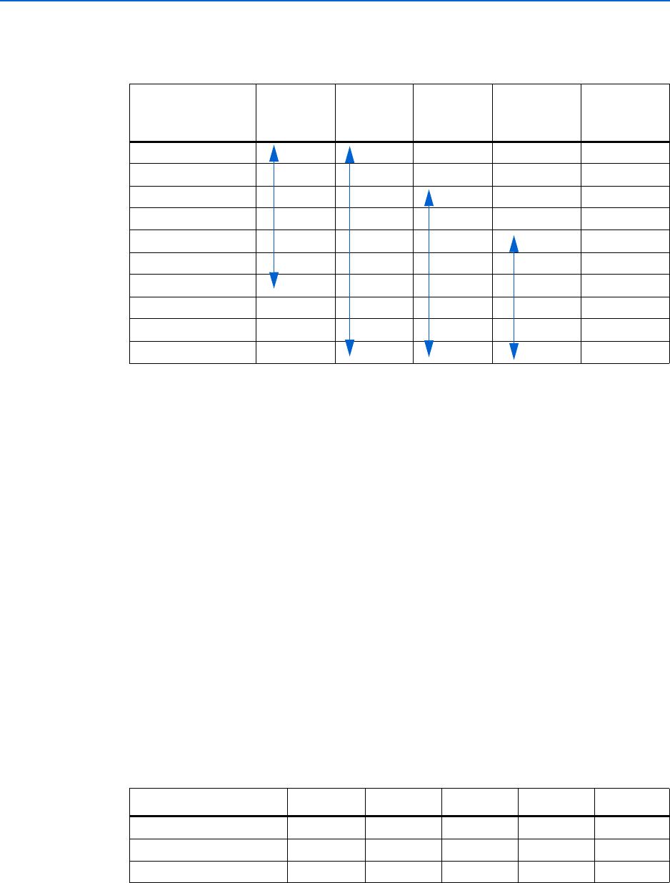
EP3SE260
Commercial
–2, –3, –4,
–4L
–2,– 3, –4,
–4L
–2, –3, –4,
–4L
Industrial (1) –3, –4, –4L –3, –4, –4L –3, –4,–4L
Note to Table 1–5:
(1) For EP3SL340, EP3SL200, and EP3SE260 devices, the industrial junction temperature range for –4L is 0–100°C, regardless of supply voltage.
Table 15. Speed Grades for Stratix III Devices (Part 2 of 2)
Device
Temperature
Grade
484 -Pin
FineLine
BGA
780-Pin
FineLine
BGA
780-Pin
Hybrid
FineLine
BGA
1152-Pin
FineLine
BGA
1152-Pin
Hybrid
FineLine
BGA
1517-Pin
FineLine
BGA
1760-Pin
FineLine
BGA

EP3SE110F1152C4L

Mfr. #:
Manufacturer:
Intel / Altera
Description:
FPGA - Field Programmable Gate Array FPGA - Stratix III 4300 LABs 744 IOs
Lifecycle:
New from this manufacturer.
Delivery:
DHL FedEx Ups TNT EMS
Payment:
T/T Paypal Visa MoneyGram Western Union