Document Number: 91055
www.vishay.com
S11-1049-Rev. C, 30-May-11 1
This document is subject to change without notice.
THE PRODUCTS DESCRIBED HEREIN AND THIS DOCUMENT ARE SUBJECT TO SPECIFIC DISCLAIMERS, SET FORTH AT
www.vishay.com/doc?91000
Power MOSFET
IRF740S, SiHF740S
Vishay Siliconix
FEATURES
• Halogen-free According to IEC 61249-2-21
Definition
• Surface Mount
• Available in Tape and Reel
• Dynamic dV/dt Rating
• Repetitive Avalanche Rated
•Fast Switching
• Ease of Paralleling
• Simple Drive Requirements
• Compliant to RoHS Directive 2002/95/EC
DESCRIPTION
Third generation Power MOSFETs from Vishay provide the
designer with the best combination of fast switching,
ruggedized device design, low on-resistance and
cost-effectiveness.
The D
2
PAK (TO-263) is a surface mount power package
capable of accommodating die size up to HEX-4. It provides
the highest power capability and the lowest possible
on-resistance in any existing surface mount package. The
D
2
PAK (TO-263) is suitable for high current applications
because of its low internal connection resistance and can
dissipate up to 2.0 W in a typical surface mount application.
Note
a. See device orientation.
Notes
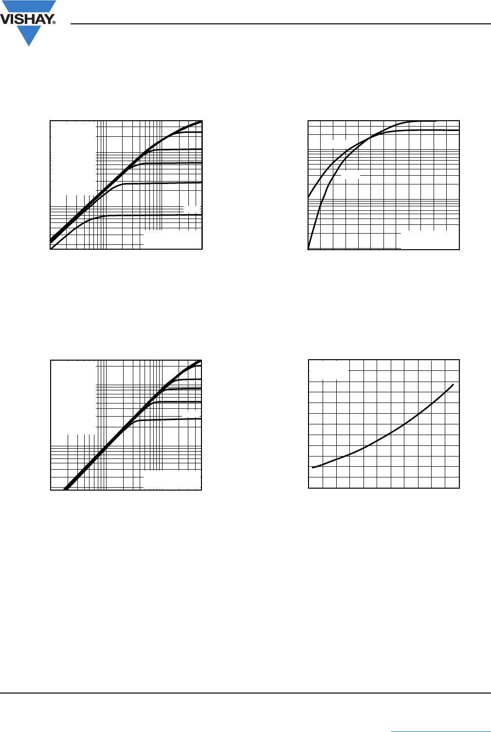
a. Repetitive rating; pulse width limited by maximum junction temperature (see fig. 11).
b. V
DD
= 50 V, starting T
J
= 25 °C, L = 9.1 mH, R
g
= 25 , I
AS
= 10 A (see fig. 12).
c. I
SD
10A, dI/dt 120 A/μs, V
DD
V
DS
, T
J
150 °C.
d. 1.6 mm from case.
e. When mounted on 1" square PCB (FR-4 or G-10 material).
PRODUCT SUMMARY
V
DS
(V) 400
R
DS(on)
()V
GS
= 10 V 0.55
Q
g
(Max.) (nC) 63
Q
gs
(nC) 9.0
Q
gd
(nC) 32
Configuration Single
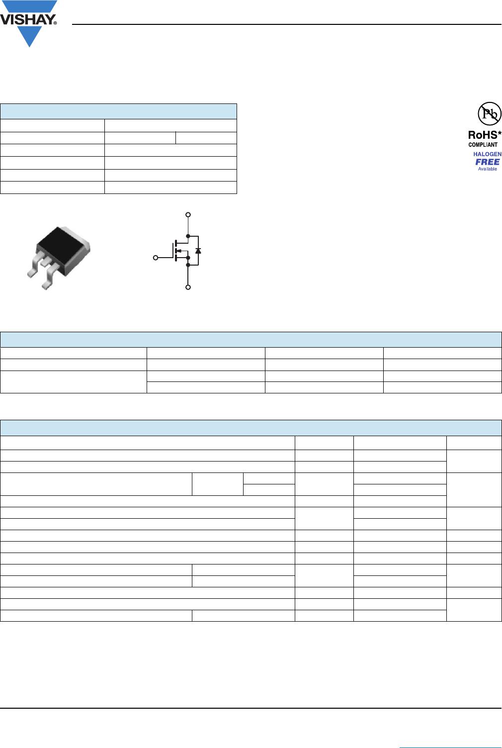
D
2
PAK (TO-263)
G
D
S
ORDERING INFORMATION
Package D
2
PAK (TO-263) D
2
PAK (TO-263) D
2
PAK (TO-263)
Lead (Pb)-free and Halogen-free SiHF740S-GE3 SiHF740STRL-GE3
a
SiHF740STRR-GE3
a
Lead (Pb)-free
IRF740SPbF IRF740STRLPbF
a
IRF740STRRPbF
a
SiHF740S-E3 SiHF740STL-E3
a
SiHF740STR-E3
a
ABSOLUTE MAXIMUM RATINGS (T
C
= 25 °C, unless otherwise noted)
PARAMETER SYMBOL LIMIT UNIT
Drain-Source Voltage V
DS
400
V
Gate-Source Voltage V
GS
± 20
Continuous Drain Current V
GS
at 10 V
T
C
= 25 °C
I
D
10
AT
C
= 100 °C 6.3
Pulsed Drain Current
a
I
DM
40
Linear Derating Factor 1.0
W/°C
Linear Derating Factor (PCB Mount)
e
0.025
Single Pulse Avalanche Energy
b
E
AS
520 mJ
Avalanche Current
a
I
AR
10 A
Repetitive Avalanche Energy
a
E
AR
13 mJ
Maximum Power Dissipation T
C
= 25 °C
P
D
125
W
Maximum Power Dissipation (PCB Mount)
e
T
A
= 25 °C 3.1
Peak Diode Recovery dV/dt
c
dV/dt 4.0 V/ns
Operating Junction and Storage Temperature Range T
J
, T
stg
- 55 to + 150
°C
Soldering Recommendations (Peak Temperature) for 10 s 300
d
* Pb containing terminations are not RoHS compliant, exemptions may apply