Expand menu
Hello, Sign in
My Account
0
Cart
Home
Products
Sensors
Semiconductors
Passive Components
Connectors
Power
Electromechanical
Optoelectronics
Circuit Protection
Integrated Circuits - ICs
Main Products
Manufacturers
Blog
Services
About OMO
About Us
Contact Us
Check Stock
VNN3NV04PTR-E
P1-P3
P4-P6
P7-P9
P10-P12
P13-P15
P16-P18
P19-P21
P22-P22
Prote
ction f
eatures
VNN
3NV04
P-E, VN
S3NV04
P-E
10/22
Doc ID 15
626 Rev
. 5
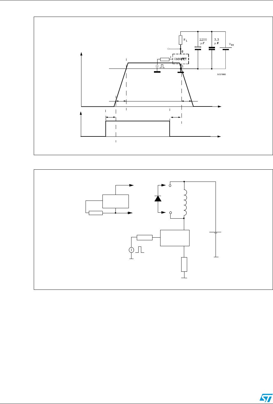
Figure
4.
Switching
time test
circuit f
or resis
tive load
Figure 5.
T
e
st circuit for diode
recovery times
R
gen
V
gen
V
D
t
I
D
90%
10%
t
V
gen
t
d(on)
t
d(off)
t
f
t
r
L=100uH
A
B
8.5
Ω
V
DD
R
gen
F
AST
DIODE
OMNIFET
A
D
I
S
220
Ω
B
OMNIFET
D
S
I
V
gen
VNN3NV04P
-E, VNS
3NV04P-E
Protecti
on features
Doc ID 15
626 Rev
. 5
1
1/22
Figure 6.
Unclamped inductiv
e load test
circuits
Figure 7.
Input charge test
circuit
Figure 8.
Unclamped induc
tive waveforms
GEN
ND8003
V
IN
Prote
ction f
eatures
VNN
3NV04
P-E, VN
S3NV04
P-E
12/22
Doc ID 15
626 Rev
. 5
3.1 Electr
ical
characteris
tics
curves
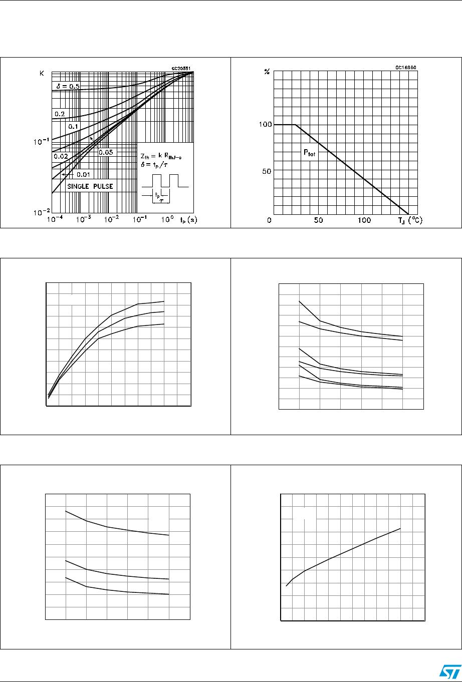
Figure 9.
Ther
mal impedance for SOT
-22
3
Figure 10.
Derating curve
Figure 1
1.
T
ransconductanc
e
Figure 12.
S
ta
tic drain-source on resist
ance
vs input voltage
(par
t 1/2)
Figur
e 13.
St
atic d
rain-sou
rce on res
istance
vs input volt
age (p
art 2/2)
Figure 14.
Source-
drain diode forward
char
acteri
stic
s
0
0.5
1
1.5
2
2.5
3
3
.5
4
4.
5
5
5.5
Id (A)
0
1
2
3
4
5
6
7
8
9
10
11
Gfs (
S)
Vds=13
V
Tj=25ºC
Tj=150ºC
Tj=-40ºC
3
3.5
4
4.5
5
5.5
6
6
.5
Vin(V)
0
25
50
75
100
125
150
175
200
225
250
275
300
Rds(on) (mohm
s)
Id=3.5A
Id=1A
Id=3.5A
Id=1A
Id=3
.5A
Id=1
A
Tj=2
5ºC
Tj=150ºC
Tj=-
40ºC
33
.
5
44
.
5
55
.
5
6
6
.
5
Vin(V)
0
25
50
75
100
125
150
175
200
225
250
Rds(on) (mohms
)
Id=
1.5A
Tj=150
ºC
Tj=-40ºC
Tj=25ºC
0
1
23456789
1
0
1
1
1
2
Id (A)
600
650
700
750
800
850
900
950
1000
1050
1100
Vsd (
mV)
Vin=0V
P1-P3
P4-P6
P7-P9
P10-P12
P13-P15
P16-P18
P19-P21
P22-P22
VNN3NV04PTR-E
Mfr. #:
Buy VNN3NV04PTR-E
Manufacturer:
STMicroelectronics
Description:
Gate Drivers OMNIFET III Low Side 120mOhm 3.5A 40V
Lifecycle:
New from this manufacturer.
Delivery:
DHL
FedEx
Ups
TNT
EMS
Payment:
T/T
Paypal
Visa
MoneyGram
Western
Union
Products related to this Datasheet
VNN3NV04PTR-E
VNS3NV04PTR-E