VCUT0505B-HD1-GS08

VCUT0505B-HD1
www.vishay.com
Vishay Semiconductors
Rev. 2.0, 08-Jun-16
1
Document Number: 81852
For technical questions, contact: ESDprotection@vishay.com
THIS DOCUMENT IS SUBJECT TO CHANGE WITHOUT NOTICE. THE PRODUCTS DESCRIBED HEREIN AND THIS DOCUMENT
ARE SUBJECT TO SPECIFIC DISCLAIMERS, SET FORTH AT www.vishay.com/doc?91000
Bidirectional Symmetrical (BiSy) Single Line ESD-Protection Diode
in LLP1006-2L
MARKING (example only)
Bar = pin 1marking
X = date code
Y = type code (see table below)
FEATURES
Ultra compact LLP1006-2L package
Low package profile < 0.4 mm
1-line ESD-protection
Working range ± 5 V
Low leakage current I
R
< 0.1 μA
Low load capacitance C
D
= 18 pF
ESD-protection acc. IEC 61000-4-2
± 20 kV contact discharge
± 25 kV air discharge
Soldering can be checked by standard vision inspection;
no X-ray necessary
Pin plating NiPdAu (e4) no whisker growth
e4 - precious metal (e.g. Ag, Au, NiPd, NiPdAu) (no Sn)
Material categorization: for definitions of compliance
please see www.vishay.com/doc?99912
PATENT(S): www.vishay.com/patents
This Vishay product is protected by one or more United States and International patents.
20855
21129
1
2
21121
XY
ORDERING INFORMATION
DEVICE NAME ORDERING CODE
TAPED UNITS PER REEL
(8 mm TAPE on 7" REEL)
MINIMUM ORDER QUANTITY
VCUT0505B-HD1 VCUT0505B-HD1-GS08 8000 8000
PACKAGE DATA
DEVICE NAME
PACKAGE
NAME
TYPE
CODE
WEIGHT
MOLDING COMPOUND
FLAMMABILITY RATING
MOISTURE
SENSITIVITY LEVEL
SOLDERING
CONDITIONS
VCUT0505B-HD1 LLP1006-2L L 0.72 mg UL 94 V-0
MSL level 1
(according J-STD-020)
260 °C/10 s at terminals
ABSOLUTE MAXIMUM RATINGS VCUT0505B-HD1
PARAMETER TEST CONDITIONS SYMBOL VALUE UNIT
Peak pulse current Acc. IEC 61000-4-5; t
p
= 8/20 μs; single shot I
PPM
3.5 A
Peak pulse power
Pin 1 to pin 2
acc. IEC 61000-4-5; t
p
= 8/20 μs; single shot
P
PP
56 W
ESD immunity
Contact discharge acc. IEC 61000-4-2; 10 pulses
V
ESD
± 20 kV
Air discharge acc. IEC 61000-4-2; 10 pulses ± 25 kV
Operating temperature Junction temperature T
J
-40 to +125 °C
Storage temperature T
stg
-55 to +150 °C
VCUT0505B-HD1
www.vishay.com
Vishay Semiconductors
Rev. 2.0, 08-Jun-16
2
Document Number: 81852
For technical questions, contact: ESDprotection@vishay.com
THIS DOCUMENT IS SUBJECT TO CHANGE WITHOUT NOTICE. THE PRODUCTS DESCRIBED HEREIN AND THIS DOCUMENT
ARE SUBJECT TO SPECIFIC DISCLAIMERS, SET FORTH AT www.vishay.com/doc?91000
CUT THE SPIKES WITH VCUT0505B-HD1:
The VCUT0505B-HD1 is a bidirectional and symmetrical (BiSy) ESD-protection device which clamps positive and negative
overvoltage transients to ground. Connected between the signal or data line and the ground the VCUT0505B-HD1 offers a high
isolation (low leakage current, low capacitance) within the specified working range. Due to the short leads and small package
size of the tiny LLP1006-2L package the line inductance is very low, so that fast transients like an ESD-strike can be clamped
with minimal over- or undershoots.
TYPICAL CHARACTERISTICS (T
amb
= 25 °C, unless otherwise specified)
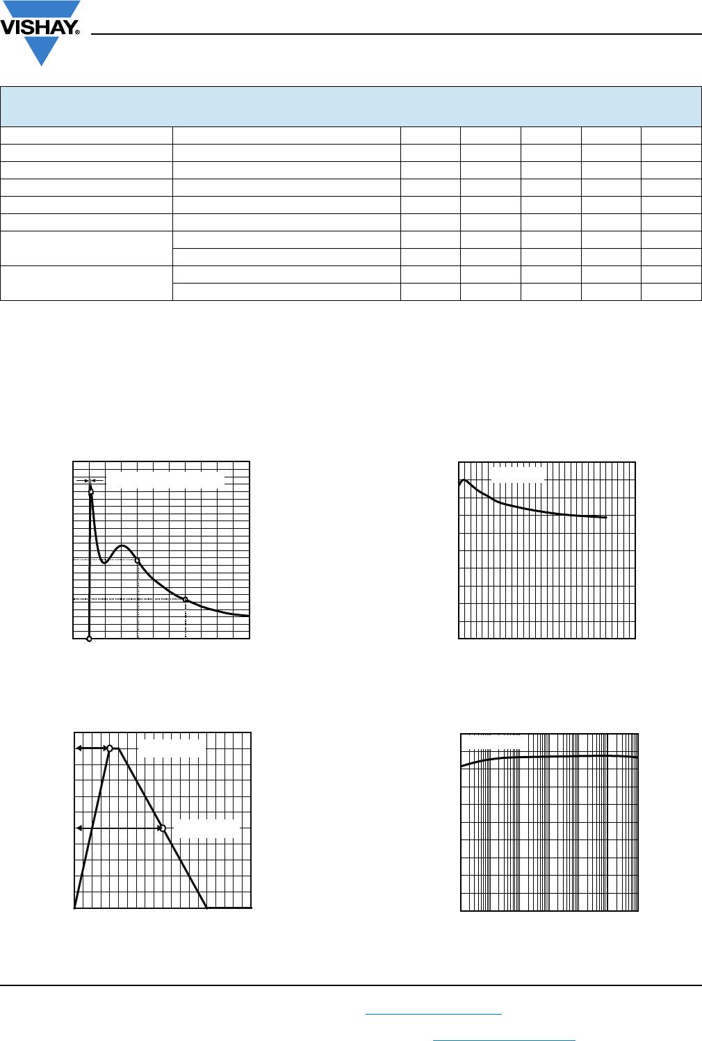
Fig. 1 - ESD Discharge Current Wave Form
acc. IEC 61000-4-2 (330 /150 pF)
Fig. 2 - 8/20 μs Peak Pulse Current Wave Form
acc. IEC 61000-4-5
Fig. 3 - Typical Capacitance C
D
vs. Reverse Voltage V
R
Fig. 4 - Typical Reverse Voltage V
R
vs. Reverse Current I
R
ELECTRICAL CHARACTERISTICS VCUT0505B-HD1
(T
amb
= 25 °C, unless otherwise specified)
PARAMETER TEST CONDITIONS/REMARKS SYMBOL MIN. TYP. MAX. UNIT
Protection paths Number of lines which can be protected N
channel
--1lines
Reverse stand-off voltage Max. reverse working voltage V
RWM
--5V
Reverse voltage at I
R
= 0.1 μA V
R
5--V
Reverse current at V
R
= 5 V I
R
--0.1μA
Reverse breakdown voltage at I
R
= 1 mA V
BR
7--V
Reverse clamping voltage
at I
PP
= 1 A V
C
--12V
at I
PP
= I
PPM
= 3.5 A V
C
--16V
Capacitance
at V
R
= 0 V; f = 1 MHz C
D
-1820pF
at V
R
= 2.5 V; f = 1 MHz C
D
-14.5- pF
0 %
20 %
40 %
60 %
80 %
100 %
120 %
-10 0 102030405060708090100
Time (ns)
Discharge Current I
ESD
Rise time = 0.7 ns to 1 ns
53 %
27 %
20557
0 %
20 %
40 %
60 %
80 %
100 %
010203040
Time (µs)
I
PPM
20 µs to 50 %
8 µs to 100 %
20548
0
2
4
6
8
10
12
14
16
18
20
0123456
V
R
(V)
C
D
(pF)
21122
f = 1 MHz
- 10
- 8
- 6
- 4
- 2
0
2
4
6
8
10
0.01 0.1 1 10 100 1000 10 000
I
R
(µA)
V
R
(V)
21123
Pin 1 to 2
VCUT0505B-HD1
www.vishay.com
Vishay Semiconductors
Rev. 2.0, 08-Jun-16
3
Document Number: 81852
For technical questions, contact: ESDprotection@vishay.com
THIS DOCUMENT IS SUBJECT TO CHANGE WITHOUT NOTICE. THE PRODUCTS DESCRIBED HEREIN AND THIS DOCUMENT
ARE SUBJECT TO SPECIFIC DISCLAIMERS, SET FORTH AT www.vishay.com/doc?91000
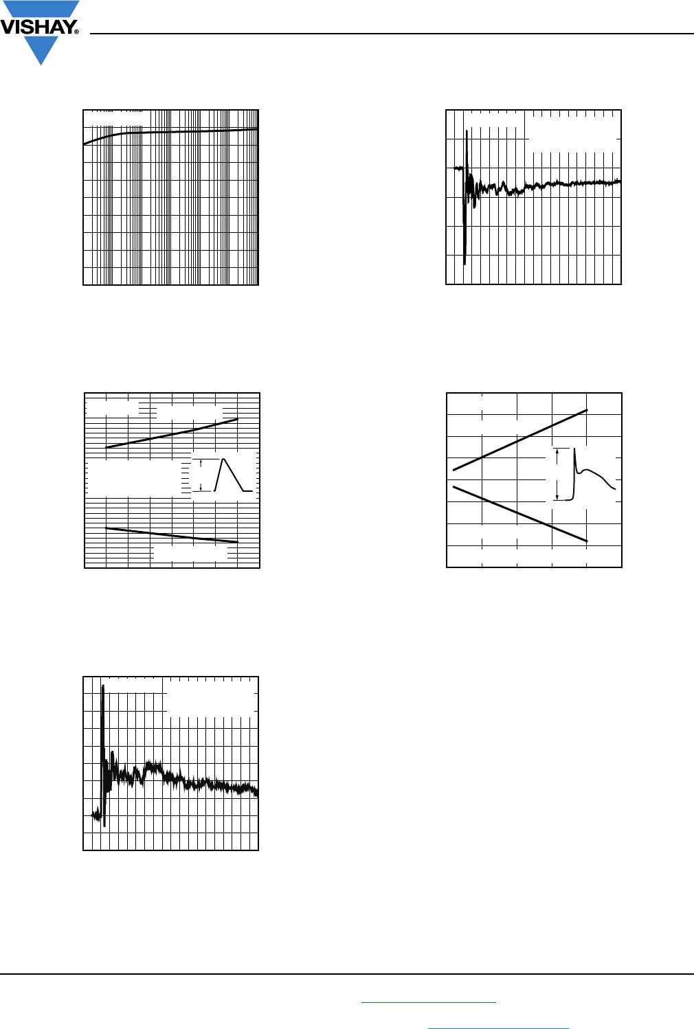
Fig. 5 - Typical Reverse Voltage V
R
vs. Reverse Current I
R
Fig. 6 - Typical Peak Clamping Voltage V
C
vs.
Peak Pulse Current I
PP
Fig. 7 - Typical Clamping Performance at + 8 kV
Contact Discharge (acc. IEC 61000-4-2)
Fig. 8 - Typical Clamping Performance at - 8 kV
Contact Discharge (acc. IEC 61000-4-2)
Fig. 9 - Typical Peak. Clamping Voltage at ESD Contact Discharge
(acc. IEC 61000-4-2)
- 10
- 8
- 6
- 4
- 2
0
2
4
6
8
10
0.01 0.1 1 10 100 1000 10 000
I
R
(µA)
V
R
(V)
21124
Pin 2 to 1
- 15
- 10
- 5
0
5
10
15
20
01234
I
PP
(A)
V
C
(V)
21125
V
C
Positive surge
Negative surge
Measured
acc. IEC 61000-4-5
(8/20 µs - wave form)
Pin 2 to 1
- 20
- 10
0
10
20
30
40
50
60
70
80
- 10 0 10 20 30 40 50 60 70 80 90
Acc. IEC 61000-4-2
+ 8 kV
contact discharge
t (ns)
V
C-ESD
(V)
21126
Pin 2 to 1
- 80
- 60
- 40
- 20
0
20
40
-100 10 2030405060708090
Acc. IEC 61000-4-2
- 8 k
V
contact discharge
t (ns)
V
C-ESD
(V)
21127
Pin 2 to 1
- 200
- 150
- 100
- 50
0
50
100
150
200
0 5 10 15 20 25
V
ESD
(kV)
V
C-ESD
(V)
21128
Acc. IEC 61000-4-2 contact discharge
V
C-ESD
Positive discharge
Negative discharge
Pin 2 to 1

VCUT0505B-HD1-GS08

Mfr. #:
Manufacturer:
Vishay Semiconductors
Description:
ESD Suppressors / TVS Diodes 5.0V 56W Single Line
Lifecycle:
New from this manufacturer.
Delivery:
DHL FedEx Ups TNT EMS
Payment:
T/T Paypal Visa MoneyGram Western Union

Products related to this Datasheet