LTC4354
7
4354fc
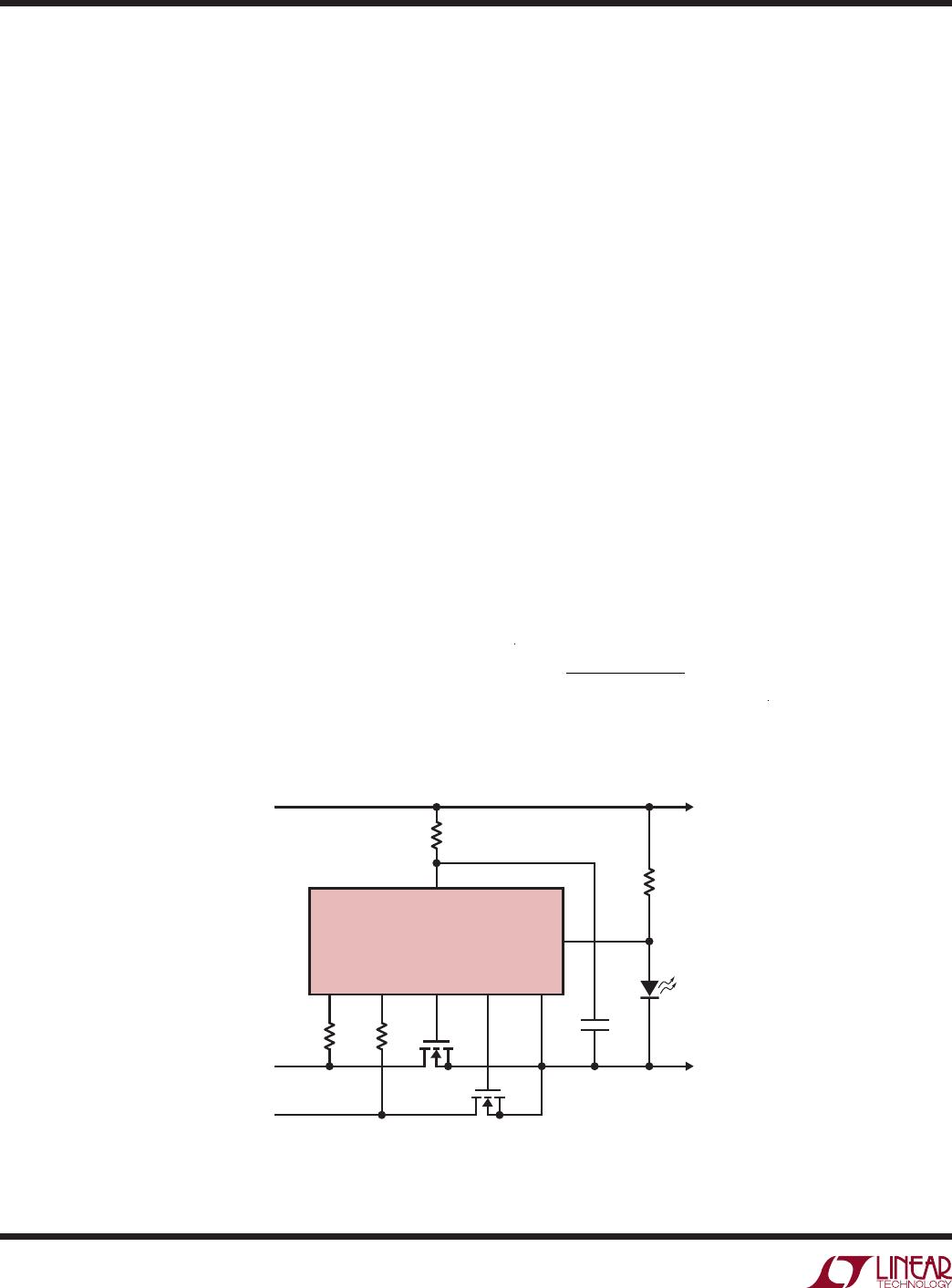
Input Power Supply
The power supply for the device is derived from –48_RTN
through an external current limiting resistor (R
IN
). An
internal shunt regulator clamps the voltage at V
CC
pin to
11V. A 1µF decoupling capacitor to V
SS
is recommended.
It also provides a soft-start to the part.
R
IN
should be chosen to accommodate the maximum
supply current requirement of 2mA at the expected input
operating voltage.
R
IN
≤
IN(MIN)
Z(MAX)
I
CC(MAX)
The power dissipation of the resistor is calculated at the
maximum DC input voltage:
P =
(V
IN(MAX)
− V
CC(MIN)
)
2
R
IN
If the power dissipation is too high for a single resistor,
use multiple low power resistors in series instead of a
single high power component.
MOSFET SELECTION
The LTC4354 drives N-channel MOSFETs to conduct the
load current. The important features of the MOSFETs are
on-resistance R
DS(ON)
, the maximum drain-source voltage
V
DSS
, and the threshold voltage.
The gate drive for the MOSFET is guaranteed to be more
than 10V and less than 12V. This allows the use of standard
threshold voltage N-channel MOSFETs. An external zener
diode can be used to clamp the potential at the V
CC
pin
to as low as 4.5V if the gate to source rated breakdown
voltage is less than 12V.
The maximum allowable drain-source voltage, V
(BR)DSS,
must be higher than the supply voltages. If the inputs are
shorted, the full supply voltage will appear across the
MOSFETs.
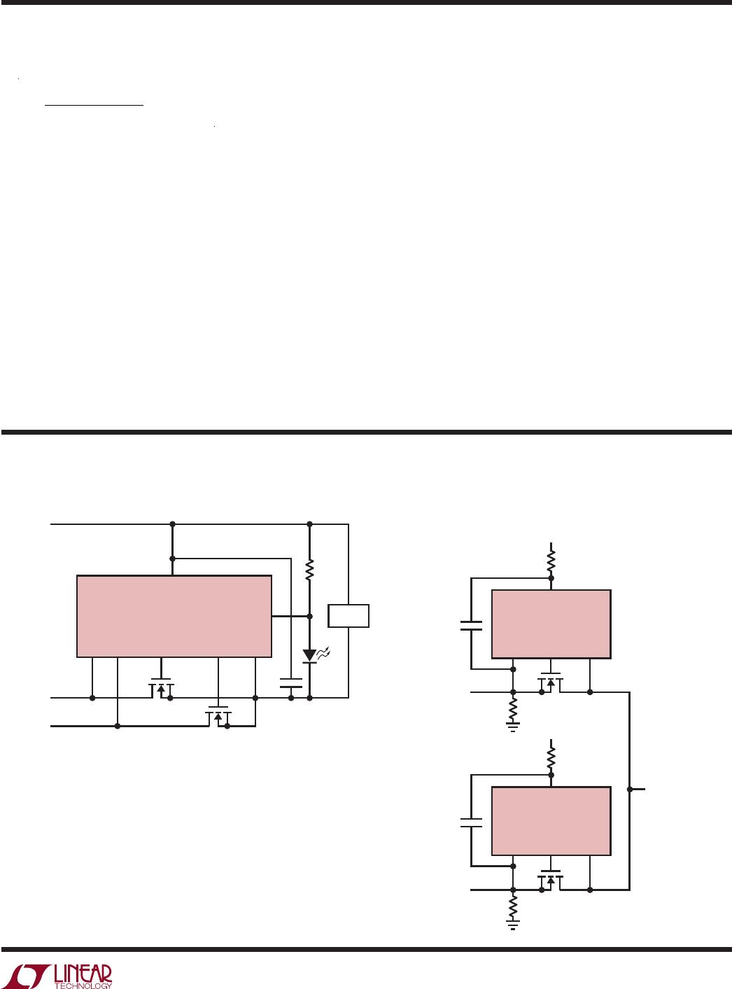
applicaTions inForMaTion
Figure 1. Method of Protecting the DA and DB Pins from
Negative Inputs. One Channel Shown
The LTC4354 tries to servo the voltage drop across the
MOSFET to 30mV in the forward direction by controlling
the gate voltage and sends out a fault signal when the
voltage drop
exceeds the 260mV fault threshold. The
R
DS(ON)
should be small enough to conduct the maximum
load current while not triggering a fault, and to stay within
the MOSFET’s power rating at the maximum load current
(I
2
• R
DS(ON)
).
Fault Conditions
LTC4354 monitors fault conditions and turns on an LED
or opto-coupler to indicate a fault. When the voltage drop
across the pass transistor is higher than the 260mV fault
threshold, the internal pull-down at the FAULT pin turns off
and allows the current to flow through the LED or opto-
coupler. Conditions that cause high voltage across the pass
transistor include: short in the load circuitry, excessive
load current, FET open while conducting current, and FET
short on the channel with the higher supply voltage. The
fault threshold is internally set to 260mV.
In the event of FET open on the channel with the more
negative supply voltage, if the voltage difference is high
enough, the substrate diode on the DA or DB pins will
forward bias. The current flowing out of the pins must
be limited to a safe level (<1mA) to prevent device latch
up. Schottky diodes can be used to
clamp the voltage at
the DA and DB pins, as shown in Figure 1.
4354 F01
DA GA
LTC4354
V
SS
MMBD2836LT1
1k
1k