P6KA16AHE3/54

P6KA6.8 thru P6KA43A
www.vishay.com
Vishay General Semiconductor
Revision: 20-Dec-13
1
Document Number: 88368
For technical questions within your region: DiodesAmericas@vishay.com
, DiodesAsia@vishay.com, DiodesEurope@vishay.com
THIS DOCUMENT IS SUBJECT TO CHANGE WITHOUT NOTICE. THE PRODUCTS DESCRIBED HEREIN AND THIS DOCUMENT
ARE SUBJECT TO SPECIFIC DISCLAIMERS, SET FORTH AT www.vishay.com/doc?91000
PAR
®
Transient Voltage Suppressors
High Temperature Stability and High Reliability Conditions
TYPICAL APPLICATIONS
Use in sensitive electronics protection against voltage
transients induced by inductive load switching and lighting
on ICs, MOSFET, signal lines of sensor units for consumer,
computer, industrial, automotive, and telecommunication.
FEATURES
Junction passivation optimized design
passivated anisotropic rectifier technology
•T
J
= 185 °C capability suitable for high reliability
and automotive requirement
Available in uni-directional polarity only
600 W peak pulse power capability with a
10/1000 μs waveform, repetitive rate (duty cycle): 0.01 %
Excellent clamping capability
Very fast response time
Low incremental surge resistance
Solder dip 275 °C max. 10 s, per JESD 22-B106
AEC-Q101 qualified
Material categorization: For definitions of compliance
please see www.vishay.com/doc?99912
MECHANICAL DATA
Case: DO-204AC, molded epoxy over passivated junction
Molding compound meets UL 94 V-0 flammability rating
Base P/NHE3 - RoHS-compliant, AEC-Q101 qualified
Terminals: Matte tin plated leads, solderable per
J-STD-002 and JESD 22-B102
HE3 suffix meets JESD 201 class 2 whisker test
Polarity: Color band denotes cathode end
Notes
(1)
Non-repetitive current pulse, per fig. 3 and derated above T
A
= 25 °C per fig. 2
(2)
Measured on 8.3 ms single half sine-wave or equivalent square wave, duty cycle = 4 per minute maximum
PRIMARY CHARACTERISTICS
V
WM
5.5 V to 36.8 V
V
BR
6.8 V to 43 V
P
PPM
600 W
P
D
5.0 W
I
FSM
75 A
T
J
max. 185 °C
Polarity Uni-directional
Package DO-204AC (DO-15)
DO-204AC (DO-15)
MAXIMUM RATINGS (T
A
= 25 °C unless otherwise noted)
PARAMETER SYMBOL VALUE UNIT
Peak pulse power dissipation with a 10/1000 μs waveform
(1)
(fig. 1) P
PPM
600 W
Pulse current with a 10/1000 μs waveform
(1)
(fig. 3) I
PPM
See next table A
Power dissipation on infinite heatsink at T
L
= 75 °C (fig. 5) P
D
5.0 W
Peak forward surge current 8.3 ms single half sine-wave
(2)
I
FSM
75 A
Maximum instantaneous forward voltage at 50 A
(2)
V
F
3.5 V
Operating junction and storage temperature range T
J
, T
STG
-65 to +185 °C
P6KA6.8 thru P6KA43A
www.vishay.com
Vishay General Semiconductor
Revision: 20-Dec-13
2
Document Number: 88368
For technical questions within your region: DiodesAmericas@vishay.com
, DiodesAsia@vishay.com, DiodesEurope@vishay.com
THIS DOCUMENT IS SUBJECT TO CHANGE WITHOUT NOTICE. THE PRODUCTS DESCRIBED HEREIN AND THIS DOCUMENT
ARE SUBJECT TO SPECIFIC DISCLAIMERS, SET FORTH AT www.vishay.com/doc?91000
Notes
(1)
Pulse test: t
p
50 ms
(2)
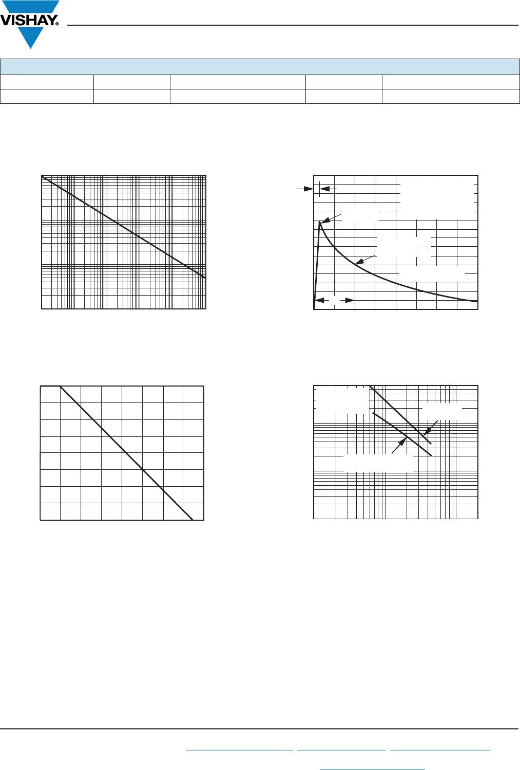
Surge current waveform per fig. 3 and derate per fig. 2
(3)
All terms and symbols are consistent with ANSI/IEEE C62.35
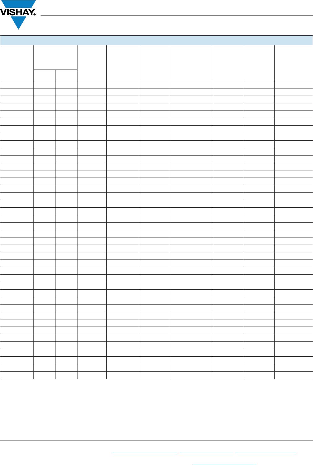
ELECTRICAL CHARACTERISTICS (T
A
= 25 °C unless otherwise noted)
DEVICE
TYPE
BREAKDOWN
VOLTAGE
V
BR
(1)
AT I
T
(V)
TEST
CURRENT
I
T
(mA)
STAND-OFF
VOLTAGE
V
WM
(V)
MAXIMUM
REVERSE
LEAKAGE
AT V
WM
I
D
(μA)
T
J
= 150 °C
MAXIMUM
REVERSE
LEAKAGE AT
V
WM
I
D
(μA)
PEAK
PULSE
CURRENT
I
PPM
(2)
(A)
MAXIMUM
CLAMPING
VOLTAGE
AT I
PPM
V
C
(V)
MAXIMUM
TEMP.
COEFFICIENT
OF V
BR
(%/°C)
MIN. MAX.
P6KA6.8 6.12 7.48 10 5.50 500 1000 55.6 10.8 0.057
P6KA6.8A 6.45 7.14 10 5.80 500 1000 57.1 10.5 0.057
P6KA7.5 6.75 8.25 10 6.05 250 500 51.3 11.7 0.061
P6KA7.5A 7.13 7.88 10 6.40 250 500 53.1 11.3 0.061
P6KA8.2 7.38 9.02 10 6.63 100 200 48.0 12.5 0.065
P6KA8.2A 7.79 8.61 10 7.02 100 200 49.6 12.1 0.065
P6KA9.1 8.19 10.0 1.0 7.37 25 50 43.5 13.8 0.068
P6KA9.1A 8.65 9.55 1.0 7.78 25 50 44.8 13.4 0.068
P6KA10 9.00 11.0 1.0 8.10 10 20 40.0 15.0 0.073
P6KA10A 9.50 10.5 1.0 8.55 10 20 41.4 14.5 0.073
P6KA11 9.90 12.1 1.0 8.92 5.0 5.0 37.0 16.2 0.075
P6KA11A 10.5 11.6 1.0 9.40 5.0 5.0 38.5 15.6 0.076
P6KA12 10.8 13.2 1.0 9.72 2.0 5.0 34.7 17.3 0.076
P6KA12A 11.4 12.6 1.0 10.2 2.0 5.0 35.9 16.7 0.078
P6KA13 11.7 14.3 1.0 10.5 2.0 5.0 31.6 19.0 0.081
P6KA13A 12.4 13.7 1.0 11.1 2.0 5.0 33.0 18.2 0.081
P6KA15 13.5 16.3 1.0 12.1 1.0 5.0 27.3 22.0 0.084
P6KA15A 14.3 15.8 1.0 12.8 1.0 5.0 28.3 21.2 0.084
P6KA16 14.4 17.6 1.0 12.9 1.0 5.0 25.5 23.5 0.086
P6KA16A 15.2 16.8 1.0 13.6 1.0 5.0 26.7 22.5 0.080
P6KA18 16.2 19.8 1.0 14.5 1.0 5.0 22.6 26.5 0.088
P6KA18A 17.1 18.9 1.0 15.3 1.0 5.0 23.8 25.2 0.088
P6KA20 18.0 22.0 1.0 16.2 1.0 5.0 20.6 29.1 0.090
P6KA20A 19.0 21.0 1.0 17.1 1.0 5.0 21.7 27.7 0.090
P6KA22 19.8 24.2 1.0 17.8 1.0 5.0 18.8 31.9 0.092
P6KA22A 20.9 23.1 1.0 18.8 1.0 5.0 19.6 30.6 0.092
P6KA24 21.6 26.4 1.0 19.4 1.0 5.0 17.3 34.7 0.094
P6KA24A 22.8 25.2 1.0 20.5 1.0 5.0 18.1 33.6 0.094
P6KA27 24.3 29.7 1.0 21.8 1.0 5.0 15.3 39.1 0.096
P6KA27A 25.7 28.4 1.0 23.1 1.0 5.0 16.0 37.5 0.096
P6KA30 27.0 33.0 1.0 24.3 1.0 5.0 13.8 43.5 0.097
P6KA30A 28.5 31.5 1.0 25.6 1.0 5.0 14.5 41.4 0.097
P6KA33 29.7 36.3 1.0 26.8 1.0 5.0 12.6 47.7 0.098
P6KA33A 31.4 34.7 1.0 28.2 1.0 5.0 13.1 45.7 0.098
P6KA36 32.4 39.6 1.0 29.1 1.0 5.0 11.5 52.0 0.099
P6KA36A 34.2 37.8 1.0 30.8 1.0 5.0 12.0 49.9 0.099
P6KA39 35.1 42.9 1.0 31.6 1.0 5.0 10.6 56.4 0.100
P6KA39A 37.1 41.0 1.0 33.3 1.0 5.0 11.1 53.9 0.100
P6KA43 38.7 47.3 1.0 34.8 1.0 5.0 9.7 61.9 0.101
P6KA43A 40.9 45.2 1.0 36.8 1.0 5.0 10.1 59.3 0.101
P6KA6.8 thru P6KA43A
www.vishay.com
Vishay General Semiconductor
Revision: 20-Dec-13
3
Document Number: 88368
For technical questions within your region: DiodesAmericas@vishay.com
, DiodesAsia@vishay.com, DiodesEurope@vishay.com
THIS DOCUMENT IS SUBJECT TO CHANGE WITHOUT NOTICE. THE PRODUCTS DESCRIBED HEREIN AND THIS DOCUMENT
ARE SUBJECT TO SPECIFIC DISCLAIMERS, SET FORTH AT www.vishay.com/doc?91000
Note
(1)
AEC-Q101 qualified
RATINGS AND CHARACTERISTICS CURVES (T
A
= 25 °C unless otherwise noted)
Fig. 1 - Peak Pulse Power Rating Curve
Fig. 2 - Pulse Power or Current vs. Initial Junction Temperature
Fig. 3 - Pulse Waveform
Fig. 4 - Typical Junction Capacitance
ORDERING INFORMATION (Example)
PREFERRED P/N UNIT WEIGHT (g) PREFERRED PACKAGE CODE BASE QUANTITY DELIVERY MODE
P6KA6.8AHE3/54
(1)
0.415 54 4000 13" diameter paper tape and reel
100
10
1
0.1
P
PPM
-
Peak Pulse Power (kW)
t
d
- Pulse Width (s)
1.0 ms
10 ms
10 μs
100 μs
0.1 μs
1.0 μs
100
75
50
25
0
0 25 50 75 100 125 150 175 200
T
J
- Initial Temperature (°C)
Peak Pulse Power (P
PP
) or Current (I
PP
)
Derating in Percentage, %
0
50
100
150
t
r
= 10 μs
Peak Value
I
PPM
Half Value -
I
PPM
I
PP
2
t
d
10/1000 μs Waveform
as defined by R.E.A.
0
1.0
2.0
3.0 4.0
t - Time (ms)
I
PPM
- Peak Pulse Current, % I
RSM
T
J
= 25 °C
Pulse Width (t
d
)
is defined as the Point
where the Peak Current
decays to 50 % of I
PPM
6000
1000
100
10
C
J
- Junction Capacitance (pF)
V
BR
- Breakdown Voltage (V)
10 1.0 100 200
Measured at
Zero Bias
Measured at Stand-Off
Voltage, V
WM
T
J
= 25 °C
f = 1.0 MHz
V
sig
= 50 mVp-p

P6KA16AHE3/54

Mfr. #:
Manufacturer:
Vishay Semiconductors
Description:
ESD Suppressors / TVS Diodes RECOMMENDED ALT 625-P6KE16AHE3
Lifecycle:
New from this manufacturer.
Delivery:
DHL FedEx Ups TNT EMS
Payment:
T/T Paypal Visa MoneyGram Western Union