10
As was the case at 2.45 GHz, the circuit is entirely dis‑
tributed element, both low cost and compact. Input
impedance for this network is given in Figure 22.
Such a circuit offers several advantages. First the voltage
outputs of two diodes are added in series, increasing
the overall value of voltage sensitivity for the network
(compared to a single diode detector). Second, the RF
impedances of the two diodes are added in parallel,
making the job of reactive matching a bit easier. Such a
circuit can easily be realized using the two series diodes
in the HSMS‑286C.
The “Virtual Battery
The voltage doubler can be used as a virtual battery,
to provide power for the operation of an I.C. or a tran‑
sistor oscillator in a tag. Illuminated by the CW signal
from a reader or inter rogator, the Schottky circuit will
produce power sufficient to operate an I.C. or to charge
up a capacitor for a burst transmis sion from an oscilla‑
tor. Where such virtual batteries are employed, the bulk,
cost, and limited lifetime of a battery are eliminated.
Temperature Compensation
The compression of the detectors transfer curve is
beyond the scope of this data sheet, but some general
comments can be made. As was given earlier, the diodes
video resistance is given by
8.33 x 10
‑5
nT
R
V
=
I
S
+ I
b
where T is the diode’s temperature in °K.
As can be seen, temperature has a strong effect upon R
V
,
and this will in turn affect video bandwidth and input
RF impedance. A glance at Figure 6 suggests that the
proper choice of bias current in the HSMS‑286x series
can minimize variation over temperature.
The detector circuits described earlier were tested
over temperature. The 915 MHz voltage doubler using
the HSMS‑286C series produced the output voltages
as shown in Figure 25. The use of 3 µA of bias resulted
in the highest voltage sensitivity, but at the cost of a
wide variation over temperature. Dropping the bias to
1 µA produced a detector with much less temperature
variation.
A similar experiment was conducted with the HSMS‑
286B series in the 5.8 GHz detector. Once again, reducing
the bias to some level under 3 µA stabilized the output
of the detector over a wide temperature range.
It should be noted that curves such as those given in
Figures 25 and 26 are highly dependent upon the exact
design of the input impedance matching network. The
designer will have to experiment with bias current using
his specific design.
HSMS-0005 fig 26 was 23
FREQUENCY (GHz): 5.6-6.0
HSMS-285X fig 27 was 24
RETURN LOSS (dB)
5.6
-20
FREQUENCY (GHz)
5.8
0
-10
-15
6.0
-5
5.9
5.7
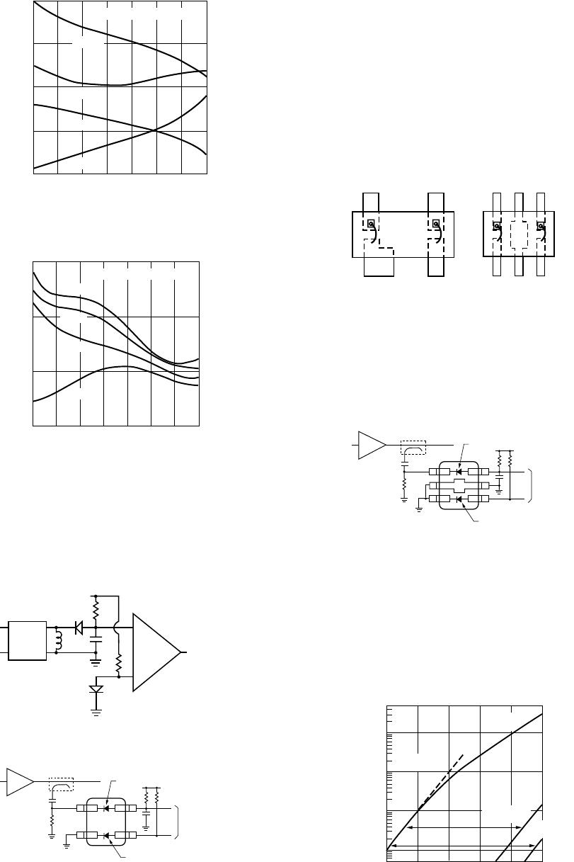
HSMS-285X fig 11 was 7
VIDEO OUT
Z-MATCH
NETWORK
RF IN
Figure 22. Input Impedance.
Input return loss, shown in Figure 23, exhibits wideband
match.
Figure 23. Input Return Loss.
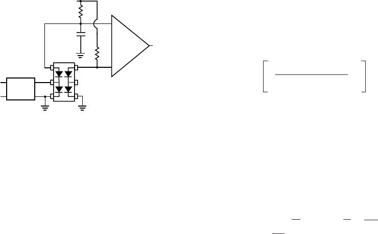
Voltage Doublers
To this point, we have restricted our discus sion to
single diode detectors. A glance at Figure 9, however,
will lead to the suggestion that the two types of single
diode detectors be combined into a two diode voltage
doubler
[4]
(known also as a full wave rectifier). Such a
detector is shown in Figure 24.
Figure 24. Voltage Doubler Circuit.
11
Figure 25. Output Voltage vs. Temperature and Bias Current
in the 915 MHz Voltage Doubler using the HSMS-286C.
in a single package, such as the SOT‑143 HSMS‑2865 as
shown in Figure 29.
In high power differential detectors, RF coupling from
the detector diode to the reference diode produces a
rectified voltage in the latter, resulting in errors.
Isolation between the two diodes can be obtained
by using the HSMS‑286K diode with leads 2 and 5
grounded. The difference between this product and the
conventional HSMS‑2865 can be seen in Figure 29.
-55 -35 -15 5 8545 65
OUTPUT VOLTAGE (mV)
TEMPERATURE (
°
C)
25
40
80
60
120
100
INPUT POWER = –30 dBm
3.0 µA
1.0 µA
10 µA
0.5 µA
OUTPUT VOLTAGE (mV)
TEMPERATURE (
°
C)
5
15
35
25
INPUT POWER = –30 dBm
3.0 µA
10 µA
1.0 µA
0.5 µA
-55 -35 -15 5 8545 6525
matching
network
differential
amplifier
bias
to differential
amplifier
V
s
detector
diode
reference diode
PA
HSMS-2865
Figure 26. Output Voltage vs. Temperature and Bias Current
in the 5.80 GHz Voltage Detector using the HSMS-286B Schottky.
Six Lead Circuits
The differential detector is often used to provide temper‑
ature compensation for a Schottky detector, as shown in
Figures 27 and 28.
Figure 27. Differential Detector.
Figure 28. Conventional Differential Detector.
These circuits depend upon the use of two diodes
having matched V
f
characteristics over all operating
temperatures. This is best achieved by using two diodes
HSMS-2865
SOT-143
HSMS-286K
SOT-363
3 4
6 5 4
11 2 2 3
to differential
amplifier
V
s
detector
diode
reference diode
PA
HSMS-286K
-35 -25 -15 -5 155
37 dB
47 dB
OUTPUT VOLTAGE (mV)
INPUT POWER (dBm)
0.5
1000
100
10
1
5000
Frequency = 900 MHz
HSMS-2825
ref. diode
RF diode
V
out
Square law
response
HSMS-282K
ref. diode
Figure 29. Comparing Two Diodes.
The HSMS‑286K, with leads 2 and 5 grounded, offers
some isolation from RF coupling between the diodes.
This product is used in a differential detector as shown
in Figure 30.
Figure 30. High Isolation Differential Detector.
In order to achieve the maximum isolation, the designer
must take care to minimize the distance from leads 2
and 5 and their respective ground via holes.
Tests were run on the HSMS‑282K and the conventional
HSMS‑2825 pair, which compare with each other in the
same way as the HSMS‑2865 and HSMS‑286K, with the
results shown in Figure 31.
Figure 31. Comparing HSMS-282K with HSMS-2825.
12
The line marked “RF diode, V
out
is the transfer curve for
the detector diode both the HSMS‑2825 and the HSMS‑
282K exhibited the same output voltage. The data were
taken over the 50 dB dynamic range shown. To the right
is the output voltage (transfer) curve for the reference
diode of the HSMS‑2825, showing 37 dB of isolation. To
the right of that is the output voltage due to RF leakage
for the reference diode of the HSMS‑282K, demonstrating
10 dB higher isolation than the conventional part.
Such differential detector circuits generally use single
diode detectors, either series or shunt mounted diodes.
The voltage doubler offers the advantage of twice
the output voltage for a given input power. The two
concepts can be combined into the differential voltage
doubler, as shown in Figure 32.
P
RF
= RF power dissipated
Note that θ
jc
, the thermal resistance from diode junction
to the foot of the leads, is the sum of two component
resistances,
matching
network
bias
differential
amplifier
Figure 32. Differential Voltage Doubler, HSMS-286P.
Here, all four diodes of the HSMS‑286P are matched in
their V
f
characteristics, because they came from adjacent
sites on the wafer. A similar circuit can be realized using
the HSMS‑286R ring quad.
Other configurations of six lead Schottky products can
be used to solve circuit design problems while saving
space and cost.
Thermal Considerations
The obvious advantage of the SOT‑363 over the SOT
143 is combination of smaller size and two extra leads.
However, the copper leadframe in the SOT‑323 and SOT
363 has a thermal conductivity four times higher than
the Alloy 42 leadframe of the SOT‑23 and SOT‑143, which
enables it to dissipate more power.
The maximum junction temperature for these three
families of Schottky diodes is 150°C under all operating
conditions. The following equation, equation 1, applies
to the thermal analysis of diodes:
11600 (V
f
- I
f
R
s
)
nT
I
f
= I
S
e - 1
Equation (3).
2 1 1
n
- 4060
(
T
-
298
)
I
s
= I
0
(
T
)
e
298
Equation (4).
T
j
= (V
f
I
f
+ P
RF
) θ
jc
+ T
a
Equation (1).
θ
jc
= θ
pkg
+ θ
chip
Equation (2).
11600 (V
f
- I
f
R
s
)
nT
I
f
= I
S
e - 1
Equation (3).
2 1 1
n
- 4060
(
T
-
298
)
I
s
= I
0
(
T
)
e
298
Equation (4).
T
j
= (V
f
I
f
+ P
RF
) θ
jc
+ T
a
Equation (1).
θ
jc
= θ
pkg
+ θ
chip
Equation (2).
11600 (V
f
- I
f
R
s
)
nT
I
f
= I
S
e - 1
Equation (3).
2 1 1
n
- 4060
(
T
-
298
)
I
s
= I
0
(
T
)
e
298
Equation (4).
T
j
= (V
f
I
f
+ P
RF
) θ
jc
+ T
a
Equation (1).
θ
jc
= θ
pkg
+ θ
chip
Equation (2).
11600 (V
f
- I
f
R
s
)
nT
I
f
= I
S
e - 1
Equation (3).
2 1 1
n
- 4060
(
T
-
298
)
I
s
= I
0
(
T
)
e
298
Equation (4).
T
j
= (V
f
I
f
+ P
RF
) θ
jc
+ T
a
Equation (1).
θ
jc
= θ
pkg
+ θ
chip
Equation (2).
where
T
j
= junction temperature
T
a
= diode case temperature
θ
jc
= thermal resistance
V
f
I
f
= DC power dissipated
Package thermal resistance for the SOT‑323 and SOT‑363
package is approximately 100°C/W, and the chip thermal
resistance for these three families of diodes is approxi‑
mately 40°C/W. The designer will have to add in the
thermal resistance from diode case to ambient a poor
choice of circuit board material or heat sink design can
make this number very high.
Equation (1) would be straightforward to solve but
for the fact that diode forward voltage is a function of
temperature as well as forward current. The equation,
equation 3, for V
f
is:
where
n = ideality factor
T = temperature in °K
R
s
= diode series resistance
and I
S
(diode saturation current) is given by
Equations (1) and (3) are solved simultaneously to obtain
the value of junction temperature for given values of
diode case temperature, DC power dissipation and RF
power dissipation.

HSMS-286K-BLKG

Mfr. #:
Manufacturer:
Broadcom / Avago
Description:
RF Detector 4 VBR 0.3 pF
Lifecycle:
New from this manufacturer.
Delivery:
DHL FedEx Ups TNT EMS
Payment:
T/T Paypal Visa MoneyGram Western Union