ISL9000A
7
FN6391.3
October 15, 2015
Submit Document Feedback
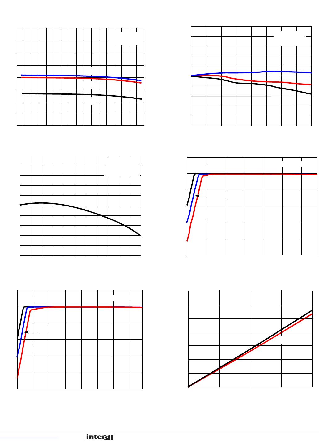
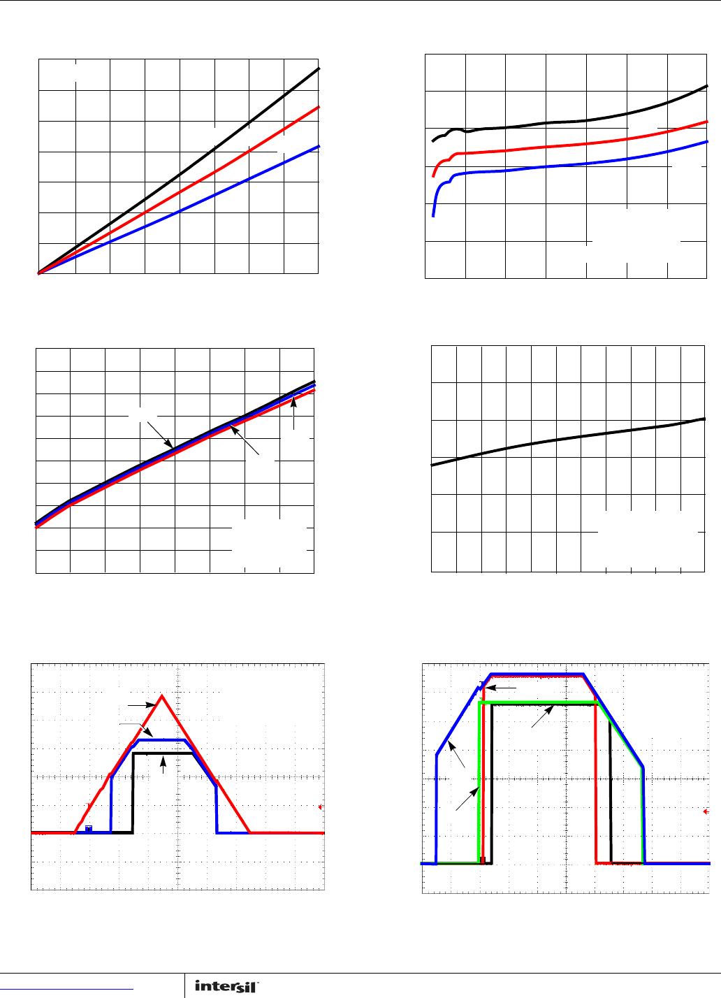
DEVICE START-UP CHARACTERISTICS
Device Enable Time t
EN
Time from assertion of the ENx pin to when the output voltage
reaches 95% of the VOx(NOM)
250 500 µs
LDO Soft-Start Ramp Rate t
SSR
Slope of linear portion of LDO output voltage ramp during start-up 30 60 µs/V
EN1, EN2 PIN CHARACTERISTICS
Input Low Voltage V
IL
-0.3 0.5 V
Input High Voltage V
IH
1.4 VIN
+
0.3
V
Input Leakage Current I
IL
, I
IH
0.1 µA
Pin Capacitance C
PIN
Informative 5 pF
POR1, POR2 PIN CHARACTERISTICS
POR1, POR2 Thresholds V
POR+
As a percentage of nominal output voltage 91 94 97 %
V
POR-
87 90 93 %
POR1
Delay t
P1LH
1.0 2.0 3.0 ms
t
P1HL
25 µs
POR2
Delay t
P2LH
C
POR
= 0.01µF 100 200 300 ms
t
P2HL
25 µs
POR1
, POR2 Pin Output Low
Voltage
V
OL
@ I
OL
= 1.0mA 0.2 V
POR1
, POR2 Pin Internal
Pull-Up Resistance
R
POR
78 100 180 k
NOTES:
6. Limits established by characterization and are not production tested.
7. VOx = 0.98*VOx(NOM); Valid for VOx greater than 1.85V.
8. Parameters with MIN and/or MAX limits are 100% tested at +25°C, unless otherwise specified. Temperature limits established by characterization
and are not production tested.
Electrical Specifications Unless otherwise noted, all parameters are guaranteed over the operational supply voltage and temperature
range of the device as follows: T
A
= -40°C to +85°C; VIN = (V
O
+ 0.5V) to 6.5V with a minimum VIN of 2.3V; C
IN
= 1µF; C
O
= 1µF; C
BYP
= 0.01µF;
C
POR
= 0.01µF. Boldface limits apply over the operating temperature range, -40°C to +85°C. (Continued)
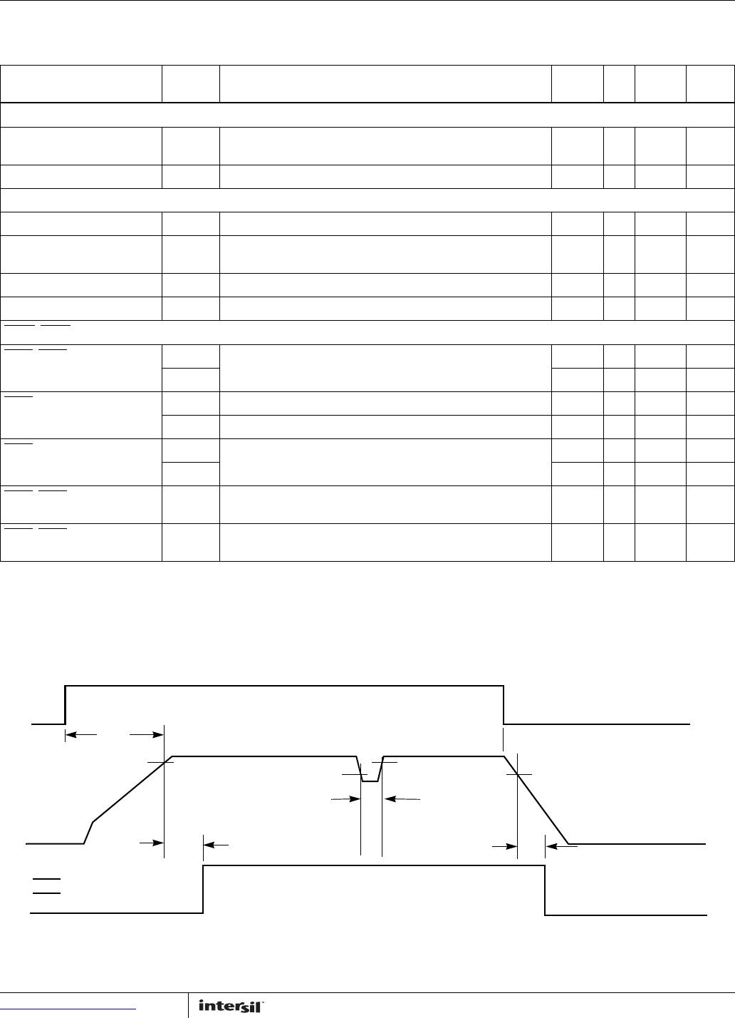
PARAMETER SYMBOL TEST CONDITIONS
MIN
(Note 8) TYP
MAX
(Note 8) UNITS
V
POR+
V
POR+
V
POR-
<t
P1HL
t
P2LH
t
P1LH
t
P1HL
t
P2HL
<t
P2HL
VO1
VO2
POR1
POR2
EN2
t
EN
V
POR-
FIGURE 2. TIMING PARAMETER DEFINITION
EN1
ISL9000A
8
FN6391.3
October 15, 2015
Submit Document Feedback
Typical Performance Curves
FIGURE 3. OUTPUT VOLTAGE vs INPUT VOLTAGE (3.3V OUTPUT) FIGURE 4. OUTPUT VOLTAGE CHANGE vs LOAD CURRENT
FIGURE 5. OUTPUT VOLTAGE CHANGE vs TEMPERATURE FIGURE 6. OUTPUT VOLTAGE vs INPUT VOLTAGE (3.3V OUTPUT)
FIGURE 7. OUTPUT VOLTAGE vs INPUT VOLTAGE (2.8V OUTPUT)
FIGURE 8. DROPOUT VOLTAGE vs LOAD CURRENT
OUTPUT VOLTAGE, VO (%)
INPUT VOLTAGE (V)
-0.6
-0.2
0.2
0.6
-0.8
3.8 4.2 6.25.8
6.63.4 4.6 5.0 5.4
-0.4
0.0
0.4
0.8
V
O
= 3.3V
+85°C
-40°C
+25°C
I
LOAD
= 0mA
0.04
0.06
-0.06
-0.10
100 200 300 4000
LOAD CURRENT - I
O
(mA)
OUTPUT VOLTAGE CHANGE (%)
-0.02
0.00
0.02
0.08
0.10
-0.04
-0.08
50 150 250 350
V
IN
= 3.8V
V
O
= 3.3V
+85°C
-40°C
+25°C
0.04
0.06
-0.06
-0.10
-10 20 50 110-40
TEMPERATURE (°C)
OUTPUT VOLTAGE CHANGE (%)
-0.02
0.00
0.02
0.08
0.10
-0.04
-0.08
-25 5 35 8065 95 125
V
IN
= 3.8V
V
O
= 3.3V
I
LOAD
= 0mA
ISL9000A
9
FN6391.3
October 15, 2015
Submit Document Feedback
FIGURE 9. DROPOUT VOLTAGE vs LOAD CURRENT FIGURE 10. GROUND CURRENT vs INPUT VOLTAGE
FIGURE 11. GROUND CURRENT vs LOAD FIGURE 12. GROUND CURRENT vs TEMPERATURE
FIGURE 13. POWER-UP/POWER-DOWN FIGURE 14. POWER-UP/POWER-DOWN WITH POR SIGNALS
Typical Performance Curves (Continued)
200
250
300
350
150
100
50
0
50 100 150 200 250 300 350 4000
OUTPUT LOAD (mA)
DROPOUT VOLTAGE, V
DO
(mV)
V
O
= 3.3V
+85°C
+25°C
-40°C
30
35
40
45
55
25
4.0 5.0 6.5
INPUT VOLTAGE (V)
GROUND CURRENT (µA)
50
3.0 3.5 4.58 5.5 6.0
I
O
(BOTH CHANNELS) = 0µA
V
O
1 = 3.3V
V
O
2 = 2.8V
-40°C
+25°C
+125°C
35
25
-10 20 50 110-40
TEMPERATURE (°C)
GROUND CURRENT (µA)
45
50
55
40
30
-25 5 35 8065 95 125
V
IN
= 3.8V
V
O
= 3.3V
I
LOAD
= 0µA
BOTH OUTPUTS ON

ISL9000AIRFDZ

Mfr. #:
Manufacturer:
Renesas / Intersil
Description:
LDO Voltage Regulators W/ANNEAL LW NOISE HI PSRRLDO 10LD 3X3 5V/
Lifecycle:
New from this manufacturer.
Delivery:
DHL FedEx Ups TNT EMS
Payment:
T/T Paypal Visa MoneyGram Western Union