74AHC86T14-13

74AHC86
Document number: DS35344 Rev. 3 - 2
1 of 8
www.diodes.com
January 2013
© Diodes Incorporated
NEW PRODUCT
74AHC86
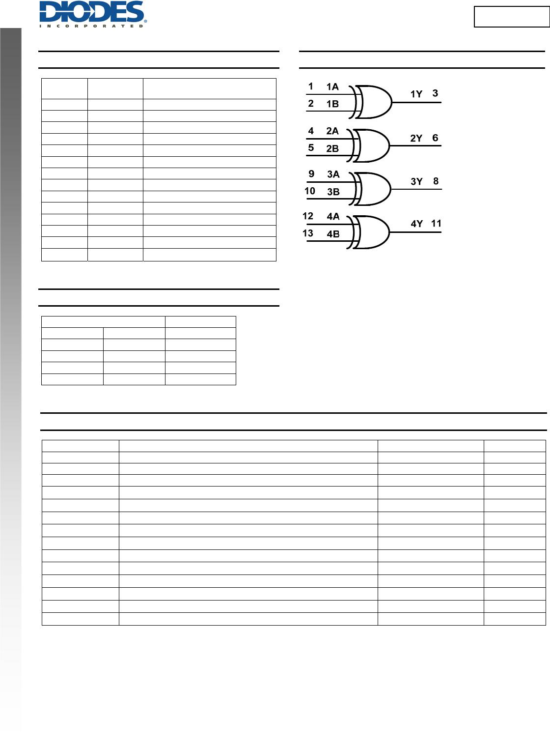
QUADRUPLE 2-INPUT EXCLUSIVE OR GATES
Description
The 74AHC86 provides provides four independent 2-input exclusive
OR gates with standard push-pull outputs. The device is designed for
operation with a power supply range of 2.0V to 5.5V. The inputs are
tolerant to 5.5V allowing this device to be used in a mixed voltage
environment.
The gates perform the Boolean function:
BAY =
or BABAY +=
Features
Wide Supply Voltage Range from 2.0V to 5.5V
Outputs Sink or Source 8mA at V
CC
= 4.5V
CMOS Low Power Consumption
Schmitt Trigger Action at All Inputs
Inputs can be driven by 3.3V or 5.5V allowing for voltage
translation applications.
ESD Protection Exceeds JESD 22
200-V Machine Model (A115-A)
2000-V Human Body Model (A114-A)
Exceeds 1000-V Charged Device Model (C101C)
Latch-Up Exceeds 250mA per JESD 78, Class II
Range of Package Options SO-14 and TSSOP-14
Totally Lead-Free & Fully RoHS Compliant (Notes 1 & 2)
Halogen and Antimony Free. “Green” Device (Note 3)
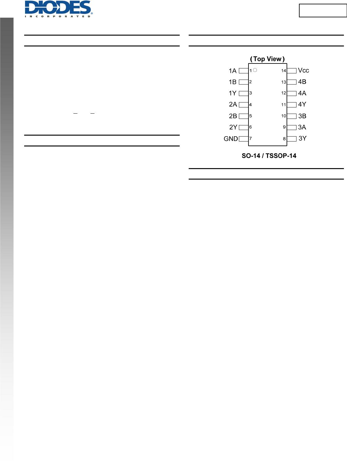
Pin Assignments
Applications
General Purpose Logic
Wide array of products such as:
PCs, Networking, Notebooks, Netbooks
Computer Peripherals, Hard Drives, CD/DVD ROM
TV, DVD, DVR, Set Top Box
Notes: 1. No purposely added lead. Fully EU Directive 2002/95/EC (RoHS) & 2011/65/EU (RoHS 2) compliant.
2. See http://www.diodes.com for more information about Diodes Incorporated’s definitions of Halogen- and Antimony-free, "Green" and Lead-free.
3. Halogen- and Antimony-free "Green” products are defined as those which contain <900ppm bromine, <900ppm chlorine (<1500ppm total Br + Cl) and
<1000ppm antimony compounds.
Click here for ordering information, located at the end of datasheet
74AHC86
Document number: DS35344 Rev. 3 - 2
2 of 8
www.diodes.com
January 2013
© Diodes Incorporated
NEW PRODUCT
74AHC86
Pin Descriptions
Pin
Number
Pin Name Function
1 1A Data Input
2 1B Data Input
3 1Y Data Output
4 2A Data Input
5 2B Data Input
6 2Y Data Output
7 GND Ground
8 3Y Data Output
9 3A Data Input
10 3B Data Input
11 4Y Data Output
12 4A Data Input
13 4B Data Input
14
V
CC
Supply Voltage
Function Table
Inputs Output
A B Y
L L L
L H H
H L H
H H L
Logic Diagram
Absolute Maximum Ratings (Note 4) (@T
A
= +25°C, unless otherwise specified.)
Symbol Description Rating Unit
ESD HBM Human Body Model ESD Protection 2 KV
ESD CDM Charged Device Model ESD Protection 1 KV
ESD MM Machine Model ESD Protection 200 V
V
CC
Supply Voltage Range -0.5 to +7.0 V
V
I
Input Voltage Range -0.5 to +7.0 V
I
IK
Input Clamp Current V
I
< -0.5V
-20 mA
I
OK
Output Clamp Current V
O
< -0.5V
-20 mA
I
OK
Output Clamp Current V
O
> V
CC
+0.5V
25 mA
I
O
Continuous Output current -0.5V < V
O
V
CC
+0.5V
+/- 25 mA
I
CC
Continuous Current Through V
CC
75 mA
I
GND
Continuous Current Through GND -75 mA
T
J
Operating Junction Temperature -40 to +150 °C
T
STG
Storage Temperature -65 to +150 °C
P
TOT
Total Power Dissipation 500 mW
Note: 4. Stresses beyond the absolute maximum may result in immediate failure or reduced reliability. These are stress values and device operation should
be within recommend values.
74AHC86
Document number: DS35344 Rev. 3 - 2
3 of 8
www.diodes.com
January 2013
© Diodes Incorporated
NEW PRODUCT
74AHC86
Recommended Operating Conditions (Note 5) (@T
A
= +25°C, unless otherwise specified.)
Symbol Parameter Conditions Min Max Unit
V
CC
Supply Voltage 2.0 5.5 V
V
I
Input Voltage 0 5.5 V
V
O
Output Voltage 0
V
CC
V
Δt/ΔV Input Transition Rise or Fall Rate
V
CC
= 3.0V to 3.6V
100
ns/V
V
CC
= 4.5V to 5.5V
20
T
A
Operating Free-Air Temperature -40 +125 °C
Note: 5. Unused inputs should be held at V
CC
or Ground.
Electrical Characteristics (@T
A
= +25°C, unless otherwise specified.)
Symbol Parameter Test Conditions
V
CC
T
A
= -40°C to +85°C T
A
= -40°C to +125°C
Unit
Min Max Min Max
V
IH
High-Level Input Voltage
2.0V 1.5 1.5
V
3.0V 2.1 2.1
5.5V 3.85 3.85
V
IL
Low-Level Input voltage
2.0V 0.5 0.5
V
3.0V 0.9 0.9
5.5V 1.65 1.65
V
OH
High-Level Output
Voltage
I
OH
= -50μA
2.0V 1.9 1.9
V
I
OH
= -50μA
3.0V 2.9 2.9
I
OH
= -50μA
4.5V 4.4 4.4
I
OH
= -4mA
3.0V 2.48 2.40
I
OH
= -8mA
4.5V 3.80 3.70
V
OL
Low-Level Output
Voltage
I
OL
= 50μA
2.0V 0.1 0.1
V
I
OL
= 50μA
3.0V 0.1 0.1
I
OL
= 50μA
4.5V 0.1 0.1
I
OL
= 4mA
3.0V 0.44 0.55
I
OL
= 8mA
4.5V 0.44 0.55
I
I
Input Current
V
I
= GND to 5.5V
3.6V ±1 ±2 μA
I
CC
Supply Current
V
I
= GND or V
CC
, I
O
= 0
3.6V 20 40 μA
Operating Characteristics
Parameter
Test
Conditions
V
CC
= 2.0V V
CC
= 3.3V V
CC
= 5V
Unit
Typ Typ Typ
C
pd
Power Dissipation
Capacitance per Gate
f = 1MHz 9.7 11.5 15.5 pF
C
i
Input Capacitance
V
i
= V
CC
– or GND
4.0 4.0 4.0 pF

74AHC86T14-13

Mfr. #:
Manufacturer:
Diodes Incorporated
Description:
Logic Gates QUAD 2-INPUT OR GATE 8mA at VCC 4.5V
Lifecycle:
New from this manufacturer.
Delivery:
DHL FedEx Ups TNT EMS
Payment:
T/T Paypal Visa MoneyGram Western Union

Products related to this Datasheet