Si8220/21
4 Rev. 1.2
1. Electrical Specifications
Table 1. Electrical Characteristics
1
V
DD
=12V or 15V, V
SS
= GND, T
A
= –40 to +125 °C; typical specs at 25 °C.
Parameter Symbol Test Conditions Min Typ Max Units
DC Specifications
Power Supply Voltage
V
DD
(V
DD
– V
SS
)6.524V
Input Current (ON)
I
F(ON)
5.0 20 mA
Input Current Rising Edge
Hysteresis
I
HYS
—0.5 mA
Input Voltage (OFF)
V
F(OFF)
Measured at ANODE with
respect to CATHODE.
0.6 1.6 V
Input Forward Voltage
V
F
Measured at ANODE with
respect to CATHODE.
I
F
=5mA.
1.7 2.5 V
Output Resistance High (Source)
R
OH
0.5 A devices 15
2.5 A devices 2.7
Output Resistance Low (Sink)
R
OL
0.5 A devices 5.0
2.5 A devices 1.0
Output High Current (Source)
I
OH
(0.5 A), I
F
=0
(see Figure 2)
—0.3
A
(2.5 A), I
F
=0
(see Figure 2)
—1.5
Output Low Current (Sink)
I
OL
(0.5 A), I
F
=10mA,
(see Figure 1)
—0.5
A
(2.5 A), I
F
=10mA,
(see Figure 1)
—2.5
High-Level Output Voltage
V
OH
(0.5 A), I
OUT
= –50 mA
V
DD
0.5
V
(2.5 A), I
OUT
= –50 mA
V
DD
0.1
Low-Level Output Voltage
V
OL
(0.5 A), I
OUT
=50mA 200
mV
(2.5 A), I
OUT
=50mA 50
High-Level Supply Current
Output open I
F
=10mA 1.2 mA
Low-Level Supply Current
Output open
V
F
= –0.6 to +1.6 V
—1.4 mA
Notes:
1. VDD = 12 V for 5, 8, and 10 V UVLO devices; VDD = 15 V for 12.5 V UVLO devices.
2. See "9.Ordering Guide" on page 22 for more information.
Si8220/21
Rev. 1.2 5
Input Reverse Voltage
BV
R
I
R
=10mA.
Measured at ANODE with
respect to CATHODE.
0.5 V
Input Capacitance
C
IN
—10 pF
VDD Undervoltage Threshold
2
VDD
UV+
V
DD
rising
5 V Threshold
See Figure 9 on page 15.
5.20 5.80 6.30
V
8 V Threshold
See Figure 10 on page 15.
7.50 8.60 9.40
V
10 V Threshold
See Figure 11 on page 15.
9.60 11.1 12.2 V
12.5 V Threshold
See Figure 12 on page 15.
12.4 13.8 14.8
VDD Undervoltage Threshold
2
VDD
UV–
V
DD
falling
5 V Threshold
See Figure 9 on page 15.
4.90 5.52 6.0 V
8 V Threshold
See Figure 10 on page 15.
7.20 8.10 8.70 V
10 V Threshold
See Figure 11 on page 15.
9.40 10.1 10.9
V
12.5 V Threshold
See Figure 12 on page 15.
11.6 12.8 13.8
VDD Lockout Hysteresis
VDD
HYS
UVLO voltage = 5 V 280 mV
VDD Lockout Hysteresis
VDD
HYS
UVLO voltage = 8 V 600 mV
VDD Lockout Hysteresis
VDD
HYS
UVLO voltage = 10 V or
12.5 V
1000 mV
AC Specifications
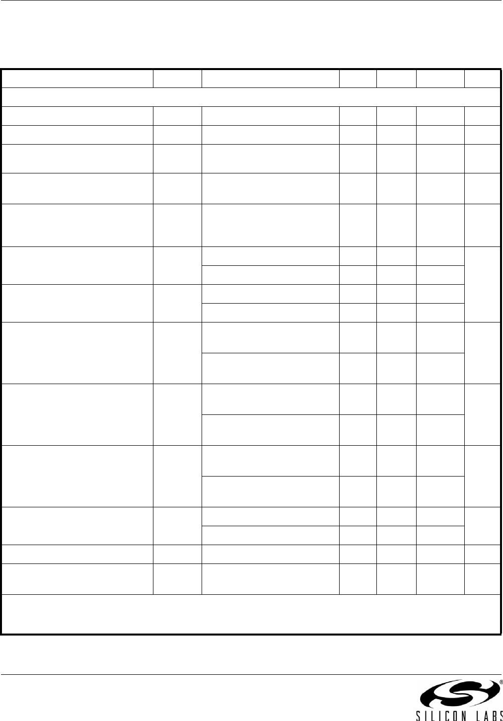
Propagation Delay Time to High
Output Level
t
PLH
C
L
= 200 pF 60 ns
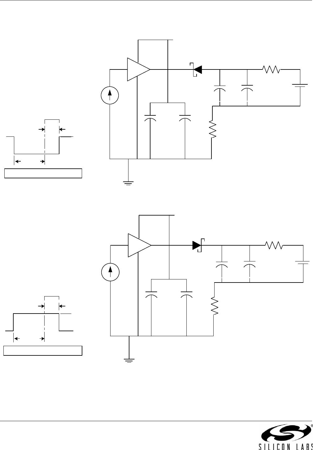
Propagation Delay Time to Low
Output Level
t
PHL
C
L
= 200 pF 40 ns
Output Rise and Fall Time
t
R
, t
F
(0.5 A), C
L
= 200 pF 30
ns
(2.5 A), C
L
= 200 pF 20
Device Startup Time
t
START
Time from
V
DD
=V
DD_UV+
to V
O
—— 40 µs
Common Mode
Transient Immunity
CMTI
Input ON or OFF
V
CM
= 1500 V (see Figure 3)
—30 kV/µs
Table 1. Electrical Characteristics (Continued)
1
V
DD
=12V or 15V, V
SS
= GND, T
A
= –40 to +125 °C; typical specs at 25 °C.
Parameter Symbol Test Conditions Min Typ Max Units
Notes:
1. VDD = 12 V for 5, 8, and 10 V UVLO devices; VDD = 15 V for 12.5 V UVLO devices.
2. See "9.Ordering Guide" on page 22 for more information.
Si8220/21
6 Rev. 1.2
2. Test Circuits
Figure 1. IOL Sink Current Test Circuit
Figure 2. IOH Source Current Test Circuit
INPUT
1 µF
100 µF
10
RSNS
0.1
Si822x
1 µF
CER
10 µF
EL
VDD = 15 V
IN OUT
VSS
VDD
SCHOTTKY
50 ns
200 ns
Measure
INPUT WAVEFORM
GND
I
F
8 V
+
_
INPUT
1 µF
100 µF
10
RSNS
0.1
Si822x
1 µF
CER
10 µF
EL
VDD = 15 V
IN OUT
VSS
VDD
50 ns
200 ns
Measure
INPUT WAVEFORM
GND
I
F
SCHOTTKY
5.5 V
+
_

SI8220DB-A-IS

Mfr. #:
Manufacturer:
Silicon Labs
Description:
Gate Drivers 2.5kV 2.5A Opto Input ISOdriver, 12.5V UVLO (HCPL3120 replacement)
Lifecycle:
New from this manufacturer.
Delivery:
DHL FedEx Ups TNT EMS
Payment:
T/T Paypal Visa MoneyGram Western Union