Si8220/21
16 Rev. 1.2
6. Applications
6.1. Power Supply Connections
V
SS
can be biased at, above, or below ground as long as the voltage on V
DD
with respect to V
SS
is a maximum of
24 V. V
DD
decoupling capacitors should be placed as close to the package pins as possible. The optimum values
for these capacitors depend on load current and the distance between the chip and its power source. It is
recommended that 0.1 and 10 µF bypass capacitors be used to reduce high-frequency noise and maximize
performance.
6.2. Layout Considerations
It is most important to minimize ringing in the drive path and noise on the V
DD
lines. Care must be taken to
minimize parasitic inductance in these paths by locating the Si8220/21 as close to the device it is driving as
possible. In addition, the V
DD
supply and ground trace paths must be kept short. For this reason, the use of power
and ground planes is highly recommended. A split ground plane system having separate ground and V
DD
planes
for power devices and small signal components provides the best overall noise performance.
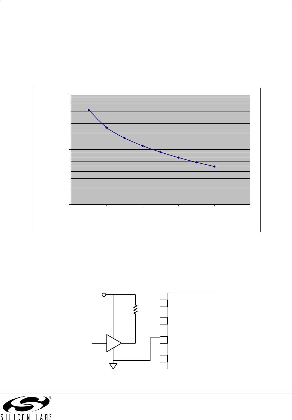
6.3. Power Dissipation Considerations
Proper system design must assure that the Si8220/21 operates within safe thermal limits across the entire load
range. The Si8220/21 total power dissipation is the sum of the power dissipated by bias supply current, internal
switching losses, and power delivered to the load, as shown in Equation 1.
Equation 1.
The maximum allowable power dissipation for the Si8220/21 is a function of the package thermal resistance,
ambient temperature, and maximum allowable junction temperature, as shown in Equation 2.
Equation 2.
Substituting values for P
Dmax
T
jmax
, T
A
, and
ja
into Equation 2 results in a maximum allowable total power
dissipation of 1.0 W. The maximum allowable load is found by substituting this limit and the appropriate datasheet
values from Table 1 on page 4 into Equation 1 and simplifying. The result is Equation 3, where V
F
=2.8V,
I
F
= 10 mA, and V
DD
=18V.
P
D
V
F
I
F
Duty CycleV
DD
I
QOUT
C
int
V
DD
2
F C
L
V
DD
2
F
where:
P
D
is the total Si8220 device power dissipation (W)
I
F
is the diode current (20 mA max)
V
F
is the diode anode voltage (2.8 V max)
I
QOUT
is the driver maximum bias curent (5 mA)
C
int
is the internal parasitic capacitance (370 pF)
V
DD
is the driver-side supply voltage (24 V max)
F is the switching frequency (Hz)
++ +=
P
Dmax
T
jmax
T
A
–
ja
---------------------------
where:
P
Dmax
is the maximum allowable Si8220/21 power dissipation (W)
T
jmax
is the Si8220/21 maximum junction temperature (150 °C)
T
A
is the ambient temperature (°C)
ja
is the Si8220/21 package junction-to-air thermal resistance (125 °C/W)